WO2013150909A1 - 有機エレクトロルミネッセンス素子 - Google Patents
有機エレクトロルミネッセンス素子 Download PDFInfo
- Publication number
- WO2013150909A1 WO2013150909A1 PCT/JP2013/058659 JP2013058659W WO2013150909A1 WO 2013150909 A1 WO2013150909 A1 WO 2013150909A1 JP 2013058659 W JP2013058659 W JP 2013058659W WO 2013150909 A1 WO2013150909 A1 WO 2013150909A1
- Authority
- WO
- WIPO (PCT)
- Prior art keywords
- group
- light emitting
- dopant
- emitting layer
- ring
- Prior art date
Links
- 0 Cc1ccc2I=C3C=CC(*)=CC3c2c1 Chemical compound Cc1ccc2I=C3C=CC(*)=CC3c2c1 0.000 description 1
Images


Classifications
-
- C—CHEMISTRY; METALLURGY
- C09—DYES; PAINTS; POLISHES; NATURAL RESINS; ADHESIVES; COMPOSITIONS NOT OTHERWISE PROVIDED FOR; APPLICATIONS OF MATERIALS NOT OTHERWISE PROVIDED FOR
- C09K—MATERIALS FOR MISCELLANEOUS APPLICATIONS, NOT PROVIDED FOR ELSEWHERE
- C09K11/00—Luminescent, e.g. electroluminescent, chemiluminescent materials
- C09K11/06—Luminescent, e.g. electroluminescent, chemiluminescent materials containing organic luminescent materials
-
- C—CHEMISTRY; METALLURGY
- C07—ORGANIC CHEMISTRY
- C07D—HETEROCYCLIC COMPOUNDS
- C07D307/00—Heterocyclic compounds containing five-membered rings having one oxygen atom as the only ring hetero atom
- C07D307/77—Heterocyclic compounds containing five-membered rings having one oxygen atom as the only ring hetero atom ortho- or peri-condensed with carbocyclic rings or ring systems
- C07D307/78—Benzo [b] furans; Hydrogenated benzo [b] furans
-
- C—CHEMISTRY; METALLURGY
- C07—ORGANIC CHEMISTRY
- C07D—HETEROCYCLIC COMPOUNDS
- C07D471/00—Heterocyclic compounds containing nitrogen atoms as the only ring hetero atoms in the condensed system, at least one ring being a six-membered ring with one nitrogen atom, not provided for by groups C07D451/00 - C07D463/00
- C07D471/02—Heterocyclic compounds containing nitrogen atoms as the only ring hetero atoms in the condensed system, at least one ring being a six-membered ring with one nitrogen atom, not provided for by groups C07D451/00 - C07D463/00 in which the condensed system contains two hetero rings
- C07D471/04—Ortho-condensed systems
-
- C—CHEMISTRY; METALLURGY
- C07—ORGANIC CHEMISTRY
- C07F—ACYCLIC, CARBOCYCLIC OR HETEROCYCLIC COMPOUNDS CONTAINING ELEMENTS OTHER THAN CARBON, HYDROGEN, HALOGEN, OXYGEN, NITROGEN, SULFUR, SELENIUM OR TELLURIUM
- C07F13/00—Compounds containing elements of Groups 7 or 17 of the Periodic System
-
- C—CHEMISTRY; METALLURGY
- C07—ORGANIC CHEMISTRY
- C07F—ACYCLIC, CARBOCYCLIC OR HETEROCYCLIC COMPOUNDS CONTAINING ELEMENTS OTHER THAN CARBON, HYDROGEN, HALOGEN, OXYGEN, NITROGEN, SULFUR, SELENIUM OR TELLURIUM
- C07F15/00—Compounds containing elements of Groups 8, 9, 10 or 18 of the Periodic System
- C07F15/0006—Compounds containing elements of Groups 8, 9, 10 or 18 of the Periodic System compounds of the platinum group
- C07F15/0033—Iridium compounds
-
- H—ELECTRICITY
- H05—ELECTRIC TECHNIQUES NOT OTHERWISE PROVIDED FOR
- H05B—ELECTRIC HEATING; ELECTRIC LIGHT SOURCES NOT OTHERWISE PROVIDED FOR; CIRCUIT ARRANGEMENTS FOR ELECTRIC LIGHT SOURCES, IN GENERAL
- H05B33/00—Electroluminescent light sources
- H05B33/12—Light sources with substantially two-dimensional radiating surfaces
- H05B33/14—Light sources with substantially two-dimensional radiating surfaces characterised by the chemical or physical composition or the arrangement of the electroluminescent material, or by the simultaneous addition of the electroluminescent material in or onto the light source
-
- H—ELECTRICITY
- H10—SEMICONDUCTOR DEVICES; ELECTRIC SOLID-STATE DEVICES NOT OTHERWISE PROVIDED FOR
- H10K—ORGANIC ELECTRIC SOLID-STATE DEVICES
- H10K50/00—Organic light-emitting devices
-
- H—ELECTRICITY
- H10—SEMICONDUCTOR DEVICES; ELECTRIC SOLID-STATE DEVICES NOT OTHERWISE PROVIDED FOR
- H10K—ORGANIC ELECTRIC SOLID-STATE DEVICES
- H10K50/00—Organic light-emitting devices
- H10K50/10—OLEDs or polymer light-emitting diodes [PLED]
- H10K50/11—OLEDs or polymer light-emitting diodes [PLED] characterised by the electroluminescent [EL] layers
-
- H—ELECTRICITY
- H10—SEMICONDUCTOR DEVICES; ELECTRIC SOLID-STATE DEVICES NOT OTHERWISE PROVIDED FOR
- H10K—ORGANIC ELECTRIC SOLID-STATE DEVICES
- H10K85/00—Organic materials used in the body or electrodes of devices covered by this subclass
- H10K85/30—Coordination compounds
- H10K85/341—Transition metal complexes, e.g. Ru(II)polypyridine complexes
- H10K85/342—Transition metal complexes, e.g. Ru(II)polypyridine complexes comprising iridium
-
- H—ELECTRICITY
- H10—SEMICONDUCTOR DEVICES; ELECTRIC SOLID-STATE DEVICES NOT OTHERWISE PROVIDED FOR
- H10K—ORGANIC ELECTRIC SOLID-STATE DEVICES
- H10K85/00—Organic materials used in the body or electrodes of devices covered by this subclass
- H10K85/60—Organic compounds having low molecular weight
- H10K85/649—Aromatic compounds comprising a hetero atom
- H10K85/654—Aromatic compounds comprising a hetero atom comprising only nitrogen as heteroatom
-
- H—ELECTRICITY
- H10—SEMICONDUCTOR DEVICES; ELECTRIC SOLID-STATE DEVICES NOT OTHERWISE PROVIDED FOR
- H10K—ORGANIC ELECTRIC SOLID-STATE DEVICES
- H10K85/00—Organic materials used in the body or electrodes of devices covered by this subclass
- H10K85/60—Organic compounds having low molecular weight
- H10K85/649—Aromatic compounds comprising a hetero atom
- H10K85/657—Polycyclic condensed heteroaromatic hydrocarbons
- H10K85/6572—Polycyclic condensed heteroaromatic hydrocarbons comprising only nitrogen in the heteroaromatic polycondensed ring system, e.g. phenanthroline or carbazole
-
- H—ELECTRICITY
- H10—SEMICONDUCTOR DEVICES; ELECTRIC SOLID-STATE DEVICES NOT OTHERWISE PROVIDED FOR
- H10K—ORGANIC ELECTRIC SOLID-STATE DEVICES
- H10K85/00—Organic materials used in the body or electrodes of devices covered by this subclass
- H10K85/60—Organic compounds having low molecular weight
- H10K85/649—Aromatic compounds comprising a hetero atom
- H10K85/657—Polycyclic condensed heteroaromatic hydrocarbons
- H10K85/6574—Polycyclic condensed heteroaromatic hydrocarbons comprising only oxygen in the heteroaromatic polycondensed ring system, e.g. cumarine dyes
-
- C—CHEMISTRY; METALLURGY
- C09—DYES; PAINTS; POLISHES; NATURAL RESINS; ADHESIVES; COMPOSITIONS NOT OTHERWISE PROVIDED FOR; APPLICATIONS OF MATERIALS NOT OTHERWISE PROVIDED FOR
- C09K—MATERIALS FOR MISCELLANEOUS APPLICATIONS, NOT PROVIDED FOR ELSEWHERE
- C09K2211/00—Chemical nature of organic luminescent or tenebrescent compounds
- C09K2211/10—Non-macromolecular compounds
- C09K2211/1003—Carbocyclic compounds
- C09K2211/1007—Non-condensed systems
-
- C—CHEMISTRY; METALLURGY
- C09—DYES; PAINTS; POLISHES; NATURAL RESINS; ADHESIVES; COMPOSITIONS NOT OTHERWISE PROVIDED FOR; APPLICATIONS OF MATERIALS NOT OTHERWISE PROVIDED FOR
- C09K—MATERIALS FOR MISCELLANEOUS APPLICATIONS, NOT PROVIDED FOR ELSEWHERE
- C09K2211/00—Chemical nature of organic luminescent or tenebrescent compounds
- C09K2211/10—Non-macromolecular compounds
- C09K2211/1018—Heterocyclic compounds
- C09K2211/1025—Heterocyclic compounds characterised by ligands
- C09K2211/1029—Heterocyclic compounds characterised by ligands containing one nitrogen atom as the heteroatom
-
- C—CHEMISTRY; METALLURGY
- C09—DYES; PAINTS; POLISHES; NATURAL RESINS; ADHESIVES; COMPOSITIONS NOT OTHERWISE PROVIDED FOR; APPLICATIONS OF MATERIALS NOT OTHERWISE PROVIDED FOR
- C09K—MATERIALS FOR MISCELLANEOUS APPLICATIONS, NOT PROVIDED FOR ELSEWHERE
- C09K2211/00—Chemical nature of organic luminescent or tenebrescent compounds
- C09K2211/10—Non-macromolecular compounds
- C09K2211/1018—Heterocyclic compounds
- C09K2211/1025—Heterocyclic compounds characterised by ligands
- C09K2211/1044—Heterocyclic compounds characterised by ligands containing two nitrogen atoms as heteroatoms
-
- C—CHEMISTRY; METALLURGY
- C09—DYES; PAINTS; POLISHES; NATURAL RESINS; ADHESIVES; COMPOSITIONS NOT OTHERWISE PROVIDED FOR; APPLICATIONS OF MATERIALS NOT OTHERWISE PROVIDED FOR
- C09K—MATERIALS FOR MISCELLANEOUS APPLICATIONS, NOT PROVIDED FOR ELSEWHERE
- C09K2211/00—Chemical nature of organic luminescent or tenebrescent compounds
- C09K2211/10—Non-macromolecular compounds
- C09K2211/1018—Heterocyclic compounds
- C09K2211/1025—Heterocyclic compounds characterised by ligands
- C09K2211/1092—Heterocyclic compounds characterised by ligands containing sulfur as the only heteroatom
-
- C—CHEMISTRY; METALLURGY
- C09—DYES; PAINTS; POLISHES; NATURAL RESINS; ADHESIVES; COMPOSITIONS NOT OTHERWISE PROVIDED FOR; APPLICATIONS OF MATERIALS NOT OTHERWISE PROVIDED FOR
- C09K—MATERIALS FOR MISCELLANEOUS APPLICATIONS, NOT PROVIDED FOR ELSEWHERE
- C09K2211/00—Chemical nature of organic luminescent or tenebrescent compounds
- C09K2211/18—Metal complexes
- C09K2211/185—Metal complexes of the platinum group, i.e. Os, Ir, Pt, Ru, Rh or Pd
-
- H—ELECTRICITY
- H10—SEMICONDUCTOR DEVICES; ELECTRIC SOLID-STATE DEVICES NOT OTHERWISE PROVIDED FOR
- H10K—ORGANIC ELECTRIC SOLID-STATE DEVICES
- H10K2101/00—Properties of the organic materials covered by group H10K85/00
- H10K2101/10—Triplet emission
-
- H—ELECTRICITY
- H10—SEMICONDUCTOR DEVICES; ELECTRIC SOLID-STATE DEVICES NOT OTHERWISE PROVIDED FOR
- H10K—ORGANIC ELECTRIC SOLID-STATE DEVICES
- H10K2101/00—Properties of the organic materials covered by group H10K85/00
- H10K2101/30—Highest occupied molecular orbital [HOMO], lowest unoccupied molecular orbital [LUMO] or Fermi energy values
Definitions
- the present invention relates to an organic electroluminescence element.
- ELD electroluminescence display
- inorganic EL elements inorganic electroluminescence elements
- organic electroluminescence elements organic EL elements
- Inorganic EL elements have been used as planar light sources, but an alternating high voltage is required to drive the light emitting elements.
- an organic EL device has a structure in which a light emitting layer containing a compound that emits light is sandwiched between a cathode and an anode, and injects electrons and holes into the light emitting layer to recombine them, thereby excitons.
- This is an element that emits light by utilizing light emission (fluorescence / phosphorescence) when the exciton is deactivated. It can emit light at a voltage of several volts to several tens of volts, and is self-luminous, so it has a wide viewing angle, high visibility, and it is a thin-film, completely solid element that saves space and portability. It is attracting attention from the viewpoint.
- Non-Patent Document 1 As the development of organic EL elements for practical use, since Princeton University has reported organic EL elements using phosphorescence emission from excited triplets (see, for example, Non-Patent Document 1), phosphorous at room temperature. Research on materials that exhibit light has become active (see, for example, Non-Patent Document 2 and Patent Document 1). In addition, recently discovered organic EL devices that use phosphorescence can realize a luminous efficiency that is approximately four times that of previous devices that use fluorescence. Research and development of light-emitting element layer configurations and electrodes are performed all over the world. For example, many compounds have been studied for synthesis centering on dopants of heavy metal complexes such as iridium complexes (see, for example, Non-Patent Document 3).
- the dopant concentration is too high, for example, when a tris body having the same ligand structure is used as the dopant, the dopants are easily stacked and concentration quenching occurs.
- concentration quenching occurs as a means for increasing the concentration of the blue dopant, for example, it is conceivable to use a hetero-body having a different ligand instead of a tris-body as a dopant of an iridium complex-based heavy metal complex. As a result, stacking of dopants is suppressed, and even if the concentration of blue dopant is high, concentration quenching does not occur, and the light emission lifetime is not expected to decrease.
- organic EL element organic electroluminescent element
- This organic EL element has a first dopant having a mixed ligand in the light emitting layer and a second dopant, and mixes two or more types of light emission of the first dopant and light emission of a second dopant different from the first dopant. This improves the color rendering of white.
- the LUMO level of the host compound contained in the light emitting layer is higher than 0.5 eV with respect to the LUMO level of the constituent material of the cathode side adjacent layer of the light emitting layer, Electrons are less likely to be injected into the light emitting layer, resulting in an increase in driving voltage, and the position where recombination of holes and electrons occurs is shifted to the cathode side interface in the light emitting layer, resulting in low luminous efficiency and lifetime performance. Is not enough.
- JP 2007-27679 A Japanese Unexamined Patent Publication No. 2011-228569
- a main object of the present invention is to provide an organic EL element that has no increase in voltage, has high luminous efficiency, and can improve the emission lifetime in a white light emitting organic EL element having at least one light emitting layer. It is to be.
- the inventors of the present invention include a dopant having a specific structure in the light emitting layer, a LUMO (H) level of the host compound of the light emitting layer, and a ligand of the dopant.
- a dopant having a specific structure in the light emitting layer
- a LUMO (H) level of the host compound of the light emitting layer and a ligand of the dopant.
- An organic electroluminescence device having at least one light emitting layer,
- the light emitting layer contains a host compound and a dopant represented by the structural formula L 1 L 2 L 3 M (where L 1 to L 3 represent a bidentate ligand and M represents a central metal).
- the LUMO (H) level of the host compound of the light emitting layer the lowest LUMO (L min ) level among the ligands L 1 to L 3 of the dopant, and the constituent material of the cathode side adjacent layer of the light emitting layer
- an organic electroluminescence device characterized in that the relationship with the LUMO (C) level of the above satisfies the conditional expressions (i) and (ii).
- an organic EL element that does not increase in voltage, has high luminous efficiency, and has improved luminous lifetime.
- the present inventors have found that the host compound and the structural formula L 1 L 2 L 3 M (L 1 to L 3 represent bidentate ligands in the light emitting layer, M represents a central metal.), And at least two arbitrarily selected ligands L 1 to L 3 of the dopant are different, and the LUMO of the host compound of the light emitting layer is different.
- the TT annihilation (triplet-triplet annihilation) is caused by the aggregation of the dopants when the dopant is in a high concentration. It is generally known that Further, in such a system, the dopant is difficult to be uniformly dispersed in the light emitting layer, and the existence distance between the dopants is increased. As a result, when the dopant is responsible for carrier transport, the carrier path is uneven and disturbed, resulting in an increase in voltage. In addition, when the host compound is responsible for carrier transport, the probability of carriers being injected into the dopant is lowered, so the recombination probability is lowered and the light emission efficiency is lowered. Further, the light emission life is reduced accordingly.
- the light emission efficiency and the light emission lifetime of the organic EL element can be improved by containing a dopant represented by the general formula (1) described later. That is, at least two arbitrarily selected ligand structures out of the plurality of ligands L 1 , L 2 , and L 3 coordinated to the central metal M are made different between the ligands between the dopants. It was found that the steric hindrance becomes stronger and the interaction between the dopants can be relaxed. Thereby, in the system in which the dopant is dispersed in the host compound in the light emitting layer of the organic EL element, the aggregation state is relaxed by relaxation of the interaction between the dopants. It is considered that the problem that the voltage rise due to the nonuniform and disturbed carrier path can be solved, and further the light emission lifetime can be reduced.
- a dopant represented by the general formula (1) described later That is, at least two arbitrarily selected ligand structures out of the plurality of ligands L 1 , L 2 , and L 3 coordinated
- the LUMO level is designed to have a specific order as described above, electrons are injected from the cathode-side adjacent layer into the host compound, not the dopant, without a barrier load. And, it is predicted that it is transported without load on the host compound occupying most of the light emitting layer. That is, it is considered that the electron transport between the dopant and the dopant is difficult, and when the electron is injected, the hole and the electron are immediately recombined. As a result, it is presumed that the region where holes and electrons recombine is not the vicinity of the interface between adjacent layers, but the central portion of the light emitting layer, and the region becomes wider.
- the dopant since the band gap of the dopant is narrower than that of the host compound, when the LUMO level is in a specific order, the dopant basically takes charge of transporting holes.
- the holes When the dopant is uniformly dispersed in the host compound, the holes are smoothly transported on the dopant, so that the holes are adjacent to the cathode side than the interface on the anode side adjacent layer (for example, hole blocking layer) side. There will be more at the interface on the layer (eg, electron transport layer) side.
- the LUMO level is in a specific order, electrons are not directly injected into the dopant from the cathode side adjacent layer side interface but are transported on the host compound, so that the recombination region is formed only at the cathode side adjacent layer interface.
- the LUMO level in the present invention is Gaussian 98 (Gaussian 98, Revision A.11.4, MJ Frisch, et al, Gaussian, Inc., Pittsburgh PA, software for molecular orbital calculation manufactured by Gaussian, USA. 2002.), and by calculating the ionization potential as a value obtained by rounding off the second decimal place of the value (eV unit conversion value) calculated by performing structural optimization using B3LYP / 6-31G * as a keyword can do.
- This calculation value is effective because the correlation between the calculation value obtained by this method and the experimental value is high.
- the value calculated as the LUMO level of the compound in which the site bonded to the metal is replaced with hydrogen was used.
- the other light emitting layer adjacent to the light emitting layer containing the dopant represented by the general formula (2) to the general formula (2-2) has a longer wavelength than the above dopant.
- the inclusion of a dopant exhibiting light emission transfers energy when the dopant represented by the general formulas (2) to (2-2) returns from the excited state to the ground state to the dopant exhibiting long wavelength light emission. From the ratio, the ratio of the dopant represented by the general formula (2) to the general formula (2-2) is more used as energy for light emission, which is preferable from the viewpoint of efficiently emitting light and improving the lifetime.
- the dopant (heterodopant) is a compound in which light emission from an excited triplet is observed, specifically, a compound that emits phosphorescence at room temperature (25 ° C.), and has a phosphorescence quantum yield of Although defined as a compound of 0.01 or more at 25 ° C., a preferred phosphorescence quantum yield is 0.1 or more.
- the phosphorescent quantum yield can be measured by the method described in Spectroscopic II, page 398 (1992 edition, Maruzen) of the Fourth Edition Experimental Chemistry Course 7.
- the energy transfer type is to obtain light emission from the phosphorescent dopant, and the other is that the phosphorescent dopant becomes a carrier trap, carrier recombination occurs on the phosphorescent dopant, and light emission from the phosphorescent dopant is obtained.
- the excited state energy of the phosphorescent dopant is required to be lower than the excited state energy of the host compound.
- the phosphorescent dopant of the present invention has a phosphorescence lifetime of less than 1.4 ⁇ sec at room temperature (25 ° C.) and a phosphorescence quantum yield of 70% or more when dispersed in the light emitting host compound of the light emitting layer.
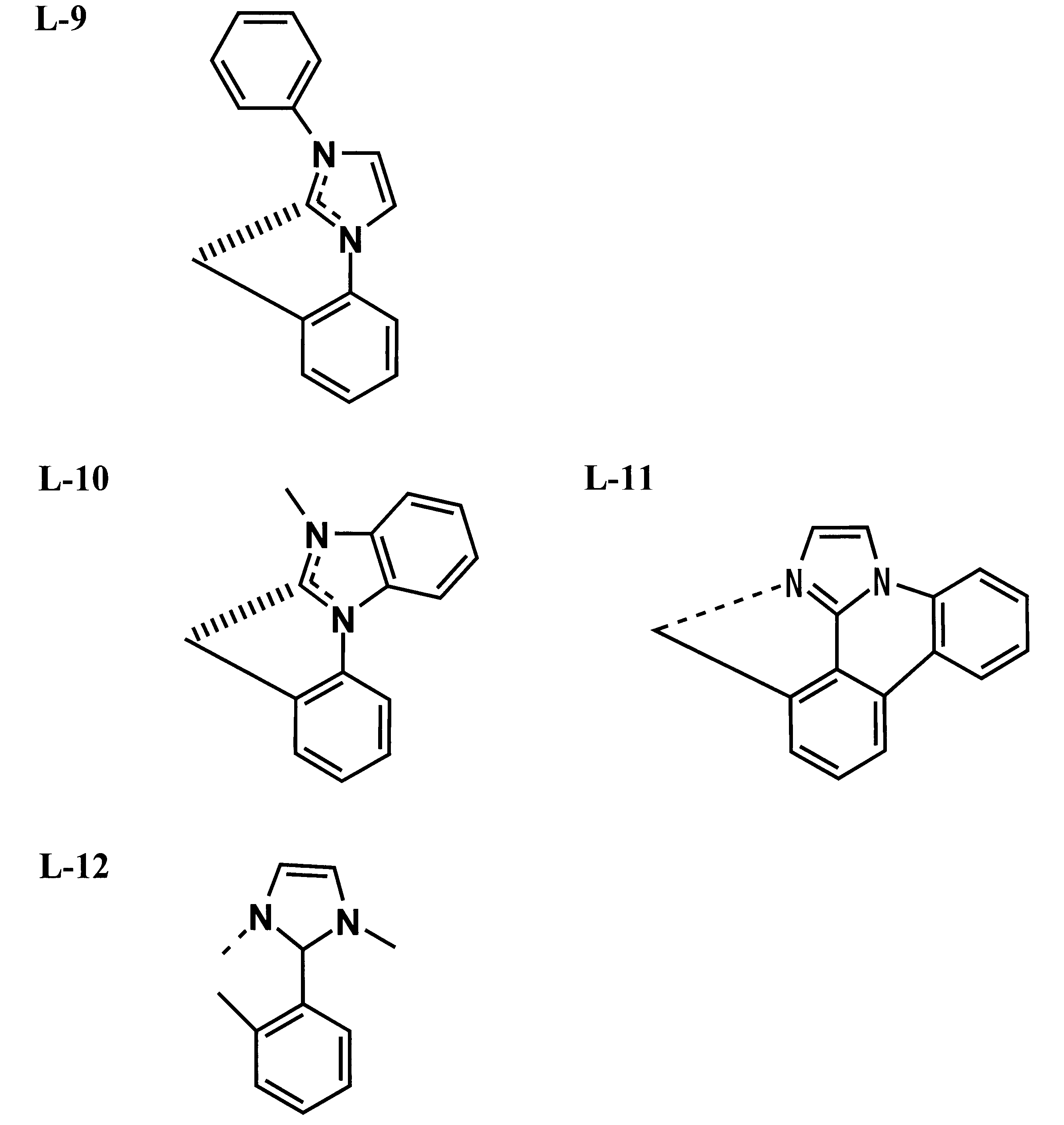
- the dopant according to the present invention is a blue phosphorescent dopant and is represented by the following general formula (1).
- L 1 to L 3 represents a bidentate ligand, and at least two arbitrarily selected among “L 1 to L 3 ” are different.
- M represents a central metal.
- Table 1 shows the LUMO levels of the above ligands.
- a preferred form of the general formula (1) is represented by the following general formula (2).
- Ring A” and “Ring B” represent a 5- or 6-membered aromatic hydrocarbon ring or aromatic heterocyclic ring.
- Ar represents an aromatic hydrocarbon ring group, an aromatic heterocyclic group, a non-aromatic hydrocarbon ring group or a non-aromatic heterocyclic group.
- R 1 ” and “R 2 ” each independently represent a hydrogen atom or a substituent, and at least one of “R 1 ” and “R 2 ” is an alkyl group or cycloalkyl group having 2 or more carbon atoms. is there.
- Ra”, “Rb” and “Rc” are each independently a hydrogen atom, halogen atom, cyano group, alkyl group, alkenyl group, alkynyl group, alkoxy group, amino group, silyl group, arylalkyl group, aryl group Represents a heteroaryl group, a non-aromatic hydrocarbon ring group or a non-aromatic heterocyclic group.
- n a and n c is 1 or 2
- n b represents an integer of 1-4.
- “L ′” is one or more of monoanionic bidentate ligands coordinated to “M”, and “M” represents a central metal.
- m ′ represents an integer of 1 or 2
- n ′ represents an integer of 1 or 2
- m ′ + n ′ is 3.
- “L ′” is a different ligand.
- R 1 and R 2 represent a substituent, it means that they may have a substituent as long as they do not impair the function of the dopant according to the present invention.
- At least one of “R 1 ” and “R 2 ” represents an alkyl group or cycloalkyl group having 2 or more carbon atoms, and the upper limit of the number of carbon atoms is within a range not impairing the function of the dopant according to the present invention. If it is, it will not specifically limit, Preferably it is C10 or less, More preferably, it is 6 or less.
- the groups represented by “Ra”, “Rb” and “Rc” may further have a substituent as long as they do not inhibit the function of the dopant according to the present invention. And the same substituents represented by “Rd ′”, “Rd ′′” and “Rd ′ ′′”.
- a preferred form of the general formula (2) is represented by the following general formula (2-1).
- “Ar” represents an aromatic hydrocarbon ring group, an aromatic heterocyclic group, a non-aromatic hydrocarbon ring group or a non-aromatic heterocyclic group.
- “R 1 ” and “R 2 ” each independently represent a hydrogen atom or a substituent, and at least one of “R 1 ” and “R 2 ” is an alkyl group or cycloalkyl group having 2 or more carbon atoms. is there.
- Ra”, “Rb” and “Rc” are each independently a hydrogen atom, halogen atom, cyano group, alkyl group, alkenyl group, alkynyl group, alkoxy group, amino group, silyl group, arylalkyl group, aryl group Represents a heteroaryl group, a non-aromatic hydrocarbon ring group or a non-aromatic heterocyclic group.
- n a and n c is 1 or 2
- n b represents an integer of 1-4.
- “L ′” is one or more of monoanionic bidentate ligands coordinated to “M”, and “M” represents a central metal.
- m ′ represents an integer of 1 or 2
- n ′ represents an integer of 1 or 2
- m ′ + n ′ is 3.
- “L ′” is a different ligand.
- R 1 and R 2 represent a substituent, it means that they may have a substituent as long as they do not impair the function of the dopant according to the present invention.
- At least one of “R 1 ” and “R 2 ” represents an alkyl group or cycloalkyl group having 2 or more carbon atoms, and the upper limit of the number of carbon atoms is within a range not impairing the function of the dopant according to the present invention. If it is, it will not specifically limit, Preferably it is C10 or less, More preferably, it is 6 or less.
- the groups represented by “Ra”, “Rb” and “Rc” may further have a substituent as long as they do not inhibit the function of the dopant according to the present invention. And the same substituents represented by “Rd ′”, “Rd ′′” and “Rd ′ ′′”.
- Rd ′”, “Rd ′′” and “Rd ′ ′′” each independently represent a linking site with another group, a hydrogen atom or a substituent, and each “Rd ′”, “Rd” ”And“ Rd ′ ′′ ”may be the same or different, and“ Rd ′ ”,“ Rd ′′ ”, and“ Rd ′ ′′ ”may be bonded to each other to form a ring.
- Rd ′ When “Rd ′”, “Rd ′′” and “Rd ′ ′′” represent a substituent, it means that the substituent may be present as long as the function of the dopant according to the present invention is not impaired.
- substituent include alkyl groups (for example, methyl group, ethyl group, propyl group, isopropyl group, tert-butyl group, pentyl group, hexyl group, octyl group, dodecyl group, tridecyl group, tetradecyl group, pentadecyl group, etc.
- Alkenyl groups eg, vinyl groups, allyl groups, etc.
- alkynyl groups eg, ethynyl groups, propargyl groups, etc.
- non-aromatic hydrocarbon ring groups eg, cycloalkyl groups (eg, cyclopentyl groups, cyclohexyl groups, etc.)
- a cycloalkoxy group eg, cyclopentyloxy group, cyclohexyloxy group, etc.
- cycloalkyl Thio group for example, cyclopentylthio group, cyclohexylthio group, etc.
- tetrahydronaphthalene ring 9,10-dihydroanthracene ring, monovalent group derived from biphenylene ring, etc.
- non-aromatic heterocyclic group for example, epoxy Ring, aziridine ring, thiirane ring, oxetane ring, a
- aromatic heterocyclic group for example, silole ring, furan ring, thiophene ring, oxazole ring, pyrrole ring, pyridine ring, pyridazine ring, pyrimidine ring, pyrazine ring, triazine ring, oxadiazole ring, triazole ring, imidazole Ring, pyrazole ring, thiazole ring, indole ring, benzimidazole ring, benzthiazole ring, benzoxazole ring, quinoxaline ring, quinazoline ring, phthalazine ring, thienothiophene ring, carbazole ring, azacarbazole ring (carbon atoms constituting carbazole ring) Any one or more of carbon atoms constituting a dibenzosilole ring, dibenzofuran ring, dibenzothiophene ring, benzothi
- M represents a central metal, and examples thereof include Os, Ir, and Pt.
- the compounds represented by the general formulas (2) and (2-1) according to the present invention can be synthesized by referring to known methods described in International Publication No. 2006-121811, etc.
- “Ar” represents an aromatic hydrocarbon ring group, an aromatic heterocyclic group, a non-aromatic hydrocarbon ring group or a non-aromatic heterocyclic group.
- “R 1 to R 4 ” each independently represents a hydrogen atom or a substituent, and at least one of “R 1 ” and “R 2 ” and at least one of “R 3 ” and “R 4 ” are each carbon.
- Ra”, “Rb”, “Ra ′” and “Rb ′” each independently represent a hydrogen atom, a halogen atom, a cyano group, an alkyl group, an alkenyl group, an alkynyl group, an alkoxy group, an amino group, a silyl group, An arylalkyl group, an aryl group, a heteroaryl group, a non-aromatic hydrocarbon ring group or a non-aromatic heterocyclic group is represented. n represents an integer of 1 or 2.
- At least one of “R 1 ” and “R 2 ” and at least one of “R 3 ” and “R 4 ” represents an alkyl group or cycloalkyl group having 2 or more carbon atoms, and the upper limit of the number of carbon atoms is The number of carbon atoms is not particularly limited as long as it does not hinder the function of the dopant according to the present invention, and it is preferably 10 or less, more preferably 6 or less.
- the group represented by “Ra”, “Rb”, “Ra ′” and “Rb ′” may further have a substituent as long as the function of the dopant according to the present invention is not impaired.
- substituents include the same substituents represented by the aforementioned “Rd ′”, “Rd ′′” and “Rd ′ ′′”.
- the host compound used in the light emitting layer is a phosphorescent phosphorous compound at a room temperature (25 ° C.) having a mass ratio of 20% or more among the compounds contained in the light emitting layer.
- a photon yield is defined as a compound of less than 0.1.
- the phosphorescence quantum yield is preferably less than 0.01.
- a host compound which can be used for this invention Although the compound conventionally used with an organic EL element can be used, The host compound with respect to the blue phosphorescence emission dopant of the light emitting layer of the organic EL element of this invention In particular, those having a structure represented by the following general formula (3) are preferable.
- X represents NR ′, O, S, CR′R ′′ or SiR′R ′′.
- R 1 represents a carbazolyl group having a phenyl group or an aromatic heterocyclic group.
- R 2 represents a carbazolyl group which may have a substituent.
- R ′ and R ′′ each independently represents a hydrogen atom or a substituent.
- R ′ and R ′′ represent a substituent, it means that the substituent may have a substituent as long as the function as a host compound according to the present invention is not impaired.
- substituents include alkyl groups (for example, methyl group, ethyl group, propyl group, isopropyl group, t-butyl group, pentyl group, hexyl group, octyl group, dodecyl group, tridecyl group, tetradecyl group, pentadecyl group).
- cycloalkyl group eg cyclopentyl group, cyclohexyl group etc.
- alkenyl group eg vinyl group, allyl group etc.
- alkynyl group eg ethynyl group, propargyl group etc.
- aromatic hydrocarbon ring group Also called aromatic carbocyclic group, aryl group, etc., for example, phenyl group, p-chlorophenyl group, mesityl group, tolyl group, Ryl group, naphthyl group, anthryl group, azulenyl group, acenaphthenyl group, fluorenyl group, phenanthryl group, indenyl group, pyrenyl group, biphenylyl group, etc.), aromatic heterocyclic group (for example, pyridyl group, pyrimidinyl group, furyl group, pyrrolyl) Group, imidazolyl group, benzoimid
- examples of the aromatic heterocyclic group contained in “R 1 ” include a pyridyl group, pyrimidinyl group, furyl group, pyrrolyl group, imidazolyl group, benzimidazolyl group, pyrazolyl group, pyrazinyl group, triazolyl group ( For example, 1,2,4-triazol-1-yl group, 1,2,3-triazol-1-yl group, etc.), oxazolyl group, benzoxazolyl group, thiazolyl group, isoxazolyl group, isothiazolyl group, furazanyl group , Thienyl group, quinolyl group, benzofuryl group, dibenzofuryl group, benzothienyl group, dibenzothienyl group, indolyl group, carbazolyl group, carbolinyl group, diazacarbazolyl group (the carbon atom constituting the carboline ring of the carboliny
- the carbazolyl group represented by “R 2 ” may have a substituent represented by R ′ and R ′′ in “X” in General Formula (3). Synonymous with group.
- X is preferably NR ′ or O
- R ′ is an aromatic hydrocarbon group (also referred to as an aromatic carbocyclic group, an aryl group, etc., for example, a phenyl group, a p-chlorophenyl group, Mesityl, tolyl, xylyl, naphthyl, anthryl, azulenyl, acenaphthenyl, fluorenyl, phenanthryl, indenyl, pyrenyl, biphenylyl) or aromatic heterocyclic groups (eg furyl, thienyl) Group, pyridyl group, pyridazinyl group, pyrimidinyl group, pyrazinyl group, triazinyl group, imidazolyl group, pyrazolyl group, thiazolyl group, quinazolinyl group, phthalazinyl group and the like are particularly preferable.
- aromatic hydrocarbon group also
- aromatic hydrocarbon group and aromatic heterocyclic group each may have a substituent represented by R ′ or R ′′ in “X” of the general formula (3).
- fluorescent dopants also referred to as fluorescent compounds
- phosphorescent dopants also referred to as phosphorescent emitters, phosphorescent compounds, phosphorescent compounds, etc.
- Fluorescent dopants include coumarin dyes, pyran dyes, cyanine dyes, croconium dyes, squalium dyes, oxobenzanthracene dyes, fluorescein dyes, rhodamine dyes, pyrylium dyes, perylene dyes, stilbene dyes , Polythiophene dyes, rare earth complex phosphors, and the like, and compounds having a high fluorescence quantum yield, such as laser dyes, are not particularly limited, and are used for the light emitting layer of an organic EL device. It can select suitably from the well-known thing to be used.
- the phosphorescent dopant is preferably a complex compound containing a group 8-10 metal in the periodic table of elements, more preferably an iridium compound, an osmium compound, a platinum compound (platinum complex compound), or a rare earth complex. Among them, the most preferable is an iridium compound.
- the other light emitting layer adjacent to the light emitting layer containing the said blue dopant contains the green dopant and red dopant which are dopants which show light emission longer wavelength than a blue dopant. It is preferable.
- the light emitting layer according to the present invention is a layer that emits light by recombination of electrons and holes injected from the electrode, the electron transport layer, or the hole transport layer. If the light emitting material (dopant) contained in the light emitting layer concerning this invention satisfy
- the total thickness of the light emitting layers in the present invention is preferably in the range of 1 to 100 nm, and more preferably 30 nm or less because a lower driving voltage can be obtained.
- the sum total of the film thickness of the light emitting layer as used in the field of this invention is a film thickness also including the said intermediate
- the film thickness of each light emitting layer is preferably adjusted in the range of 1 to 50 nm, more preferably in the range of 1 to 20 nm. There is no particular limitation on the relationship between the film thicknesses of the blue, green and red light emitting layers.
- the above-described host compound or light-emitting material is formed by forming a film by a known thinning method such as a vacuum evaporation method, a spin coating method, a casting method, an LB method, or an inkjet method. it can.
- a plurality of light emitting materials may be mixed in each light emitting layer, or a phosphorescent light emitting material and a fluorescent light emitting material may be mixed and used in the same light emitting layer.
- the constitution of the light emitting layer preferably contains a host compound and a dopant and emits light from the dopant.
- Recombination region Of the entire region of the light emitting layer, the region contributing to light emission (recombination region) can be calculated from the value of ⁇ PL / ⁇ EL and the width of the region can be estimated from the calculation result.
- ⁇ EL and ⁇ PL respectively represent the intensity decay rates of electroluminescence (EL) and photoluminescence (PL) before and after driving, and can be represented by the following equations.
- ⁇ EL 1 ⁇ [EL (after driving) / EL (before driving)]
- ⁇ PL 1 ⁇ [PL (after driving) / PL (before driving)]
- the PL value after the PL driving is measured in a state after driving the organic EL element until the light emission luminance is about half from the initial luminance ( ⁇ EL is about 0.5).
- ⁇ PL represents a recombination region with respect to the entire light emitting layer, it is estimated that the recombination region contributing to light emission is narrow when ⁇ PL / ⁇ EL is small, and light emission occurs when ⁇ PL / ⁇ EL is large. It is presumed that the recombination region contributing is wide.
- 1A to 1D are schematic views showing respective regions in the layer thickness direction of the light emitting layer 1, and the left-right direction in FIG. 1 corresponds to the layer thickness direction.
- the light emitting layer 1 is partitioned into a region contributing to light emission (recombination region 10) and a region 12 not contributing to light emission. Accordingly, the recombination region 10 is a measurement target for “EL before driving”.
- the PL before driving is the measurement target of the region 20 representing the entire light emitting layer.
- “PL after driving” indicates that the remaining region 22 obtained by subtracting the non-light-emitting region 16 from the region 20 representing the entire light-emitting layer in accordance with the formation of the non-light-emitting region 16 in the recombination region 10 is measured. It becomes.
- An injection layer is a layer provided between an electrode and an organic layer in order to reduce drive voltage and improve light emission luminance.
- Organic EL element and its forefront of industrialization (issued by NTT Corporation on November 30, 1998) 2), Chapter 2, “Electrode Materials” (pages 123 to 166) in detail, and includes a hole injection layer (anode buffer layer) and an electron injection layer (cathode buffer layer).
- the injection layer is provided as necessary, and may be present between the anode and the light emitting layer or the hole transport layer and between the cathode and the light emitting layer or the electron transport layer as described above.
- hole injection layer anode buffer layer
- hole injection layer anode buffer layer
- copper phthalocyanine is used.
- examples thereof include a phthalocyanine buffer layer represented by an oxide, an oxide buffer layer represented by vanadium oxide, an amorphous carbon buffer layer, and a polymer buffer layer using a conductive polymer such as polyaniline (emeraldine) or polythiophene.
- cathode buffer layer Details of the electron injection layer (cathode buffer layer) are also described in JP-A-6-325871, JP-A-9-17574, JP-A-10-74586, and the like. Specifically, strontium, aluminum, etc.
- Metal buffer layer typified by lithium
- alkali metal compound buffer layer typified by lithium fluoride
- alkaline earth metal compound buffer layer typified by magnesium fluoride
- oxide buffer layer typified by aluminum oxide, etc. .
- the injection layer is preferably a very thin film, and the film thickness is preferably in the range of 0.1 nm to 5 ⁇ m although it depends on the material.
- ⁇ Blocking layer hole blocking layer, electron blocking layer>
- the blocking layer is provided as necessary in addition to the basic constituent layer of the organic compound thin film as described above. For example, it is described in JP-A Nos. 11-204258 and 11-204359, and “Organic EL elements and the forefront of industrialization (published by NTT Corporation on Nov. 30, 1998)”. There is a hole blocking (hole blocking) layer.
- the hole blocking layer has a function of an electron transport layer in a broad sense, and is made of a hole blocking material having a function of transporting electrons and a very small ability to transport holes. By blocking the holes, the probability of recombination of electrons and holes can be improved. Moreover, the structure of the electron carrying layer mentioned later can be used as a hole-blocking layer concerning this invention as needed.
- the hole blocking layer of the organic EL device of the present invention is preferably provided adjacent to the light emitting layer.
- the hole blocking layer preferably contains an azacarbazole derivative.
- the light emitting layer having the shortest wavelength of light emission is preferably closest to the anode among all the light emitting layers.
- 50% by mass or more of the compound contained in the hole blocking layer provided at the position has an ionization potential of 0.3 eV or more larger than the host compound of the shortest wave emitting layer.
- the ionization potential is defined by the energy required to emit electrons at the HOMO (highest occupied molecular orbital) level of the compound to the vacuum level.
- the ionization potential is obtained by the method shown in (1) and (2) below. Can do.
- Gaussian98 (Gaussian98, Revision A.11.4, MJ Frisch, et al, Gaussian, Inc., Pittsburgh PA, 2002.), which is software for molecular orbital calculation manufactured by Gaussian, USA.
- the ionization potential can be obtained as a value obtained by rounding off the second decimal place of a value (eV unit converted value) calculated by performing structure optimization using B3LYP / 6-31G * as a keyword. This calculation value is effective because the correlation between the calculation value obtained by this method and the experimental value is high.
- the ionization potential can also be obtained by a method of direct measurement by photoelectron spectroscopy.
- a low energy electron spectrometer “Model AC-1” manufactured by Riken Keiki Co., Ltd. or a method known as ultraviolet photoelectron spectroscopy can be suitably used.
- the electron blocking layer has a function of a hole transport layer in a broad sense, and is made of a material having a function of transporting holes while having a remarkably small ability to transport electrons. The probability of recombination of electrons and holes can be improved by blocking. Moreover, the structure of the positive hole transport layer mentioned later can be used as an electron blocking layer as needed.
- the film thickness of the hole blocking layer and the electron transport layer according to the present invention is preferably 3 nm to 100 nm, more preferably 5 nm to 30 nm.
- the hole transport layer is made of a hole transport material having a function of transporting holes, and in a broad sense, a hole injection layer and an electron blocking layer are also included in the hole transport layer.
- the hole transport layer can be provided as a single layer or a plurality of layers.
- the hole transport material has any one of hole injection or transport and electron barrier properties, and may be either organic or inorganic.
- triazole derivatives oxadiazole derivatives, imidazole derivatives, polyarylalkane derivatives, pyrazoline derivatives and pyrazolone derivatives, phenylenediamine derivatives, arylamine derivatives, amino-substituted chalcone derivatives, oxazole derivatives, styrylanthracene derivatives, fluorenone derivatives, hydrazone derivatives
- Examples thereof include stilbene derivatives, silazane derivatives, aniline copolymers, and conductive polymer oligomers, particularly thiophene oligomers.
- the above-mentioned materials can be used as the hole transport material, but it is preferable to use a porphyrin compound, an aromatic tertiary amine compound and a styrylamine compound, particularly an aromatic tertiary amine compound.
- aromatic tertiary amine compounds and styrylamine compounds include N, N, N ′, N′-tetraphenyl-4,4′-diaminophenyl; N, N′-diphenyl-N, N′— Bis (3-methylphenyl)-[1,1′-biphenyl] -4,4′-diamine (TPD); 2,2-bis (4-di-p-tolylaminophenyl) propane; 1,1-bis (4-di-p-tolylaminophenyl) cyclohexane; N, N, N ′, N′-tetra-p-tolyl-4,4′-diaminobiphenyl; 1,1-bis (4-di-p-tolyl) Aminophenyl) -4-phenylcyclohexane; bis (4-dimethylamino-2-methylphenyl) phenylmethane; bis (4-di-p-tolylaminoph
- polymer materials in which these materials are introduced into polymer chains or these materials are used as polymer main chains can also be used.
- inorganic compounds such as p-type-Si and p-type-SiC can also be used as the hole injection material and the hole transport material.
- JP-A-11-251067 J. Org. Huang et. al.
- a so-called p-type hole transport material described in a book (Applied Physics Letters 80 (2002), p. 139) can also be used.
- these materials are preferably used because a light-emitting element with higher efficiency can be obtained.
- the hole transport layer is formed by thinning the hole transport material by a known method such as a vacuum deposition method, a spin coating method, a casting method, a printing method including an ink jet method, or an LB method. Can do.
- the thickness of the hole transport layer is not particularly limited, but is usually about 5 nm to 5 ⁇ m, preferably 5 nm to 200 nm.
- the hole transport layer may have a single layer structure composed of one or more of the above materials.
- a hole transport layer having a high p property doped with impurities can be used.
- examples thereof include JP-A-4-297076, JP-A-2000-196140, and JP-A-2001-102175. Appl. Phys. 95, 5773 (2004), and the like.
- the electron transport layer is made of a material having a function of transporting electrons, and in a broad sense, an electron injection layer and a hole blocking layer are also included in the electron transport layer.
- the electron transport layer can be provided as a single layer or a plurality of layers.
- electrons injected from the cathode are used.
- Any material can be used as long as it has a function of transmitting to the light-emitting layer, and any material can be selected from conventionally known compounds. For example, nitro-substituted fluorene derivatives, diphenylquinone derivatives, thiopyrans can be used.
- Dioxide derivatives, carbodiimides, fluorenylidenemethane derivatives, anthraquinodimethane and anthrone derivatives, oxadiazole derivatives and the like can be mentioned.
- a thiadiazole derivative in which the oxygen atom of the oxadiazole ring is substituted with a sulfur atom, or a quinoxaline derivative having a quinoxaline ring known as an electron withdrawing group can also be used as an electron transport material.
- a polymer material in which these materials are introduced into a polymer chain or these materials are used as a polymer main chain can also be used.
- metal complexes of 8-quinolinol derivatives such as tris (8-quinolinol) aluminum (Alq), tris (5,7-dichloro-8-quinolinol) aluminum, tris (5,7-dibromo-8-quinolinol) aluminum Tris (2-methyl-8-quinolinol) aluminum, tris (5-methyl-8-quinolinol) aluminum, bis (8-quinolinol) zinc (Znq), and the like, and the central metals of these metal complexes are In, Mg, Metal complexes replaced with Cu, Ca, Sn, Ga or Pb can also be used as the electron transport material.
- metal-free or metal phthalocyanine or those having terminal ends substituted with an alkyl group or a sulfonic acid group can be preferably used as the electron transporting material.
- the distyrylpyrazine derivative exemplified as the material for the light emitting layer can also be used as an electron transport material, and an inorganic semiconductor such as n-type-Si, n-type-SiC, etc. as in the case of the hole injection layer and the hole transport layer. Can also be used as an electron transporting material.
- the electron transport layer can be formed by thinning the electron transport material by a known method such as a vacuum deposition method, a spin coating method, a casting method, a printing method including an ink jet method, or an LB method. .
- the thickness of the electron transport layer is not particularly limited, but is usually about 5 nm to 5 ⁇ m, preferably 5 nm to 200 nm.
- the electron transport layer may have a single layer structure composed of one or more of the above materials.
- an electron transport layer having a high n property doped with impurities can also be used.
- examples thereof include JP-A-4-297076, JP-A-10-270172, JP-A-2000-196140, 2001-102175, J.A. Appl. Phys. 95, 5773 (2004), and the like.
- an electrode material made of a metal, an alloy, an electrically conductive compound and a mixture thereof having a high work function (4 eV or more) is preferably used.
- electrode substances include metals such as Au, and conductive transparent materials such as CuI, indium tin oxide (ITO), SnO 2 , and ZnO.
- conductive transparent materials such as CuI, indium tin oxide (ITO), SnO 2 , and ZnO.
- an amorphous material such as IDIXO (In 2 O 3 —ZnO) capable of forming a transparent conductive film may be used.
- a thin film may be formed by depositing these electrode materials by a method such as vapor deposition or sputtering, and a pattern having a desired shape may be formed by photolithography, or when the pattern accuracy is not so high (about 100 ⁇ m or more) ), A pattern may be formed through a mask having a desired shape when the electrode material is deposited or sputtered. Or when using the substance which can be apply
- the transmittance is greater than 10%, and the sheet resistance as the anode is preferably several hundred ⁇ / ⁇ or less.
- the film thickness depends on the material, it is usually selected in the range of 10 nm to 1000 nm, preferably 10 nm to 200 nm.
- cathode a material having a low work function (4 eV or less) metal (referred to as an electron injecting metal), an alloy, an electrically conductive compound, and a mixture thereof as an electrode material is used.
- electrode materials include sodium, sodium-potassium alloy, magnesium, lithium, magnesium / copper mixture, magnesium / silver mixture, magnesium / aluminum mixture, magnesium / indium mixture, aluminum / aluminum oxide (Al 2 O 3 ) Mixtures, indium, lithium / aluminum mixtures, rare earth metals and the like.
- a mixture of an electron injecting metal and a second metal which is a stable metal having a larger work function than this for example, a magnesium / silver mixture, Magnesium / aluminum mixtures, magnesium / indium mixtures, aluminum / aluminum oxide (Al 2 O 3 ) mixtures, lithium / aluminum mixtures, aluminum and the like are preferred.
- the cathode can be produced by forming a thin film of these electrode materials by a method such as vapor deposition or sputtering.
- the sheet resistance as a cathode is preferably several hundred ⁇ / ⁇ or less, and the film thickness is usually selected in the range of 10 nm to 5 ⁇ m, preferably 50 nm to 200 nm.
- the film thickness is usually selected in the range of 10 nm to 5 ⁇ m, preferably 50 nm to 200 nm.
- a transparent or semi-transparent cathode can be produced by producing the conductive transparent material mentioned in the description of the anode on the cathode after producing the metal with a film thickness of 1 nm to 20 nm. By applying this, an element in which both the anode and the cathode are transmissive can be manufactured.
- a support substrate (hereinafter also referred to as a substrate, substrate, substrate, support, etc.) that can be used in the organic EL device of the present invention, there is no particular limitation on the type of glass, plastic, etc., and it is transparent. May be opaque. When extracting light from the support substrate side, the support substrate is preferably transparent. Examples of the transparent support substrate preferably used include glass, quartz, and a transparent resin film. A particularly preferable support substrate is a resin film capable of giving flexibility to the organic EL element.
- polyesters such as polyethylene terephthalate (PET) and polyethylene naphthalate (PEN), polyethylene, polypropylene, cellophane, cellulose diacetate, cellulose triacetate, cellulose acetate butyrate, cellulose acetate propionate (CAP), Cellulose esters such as cellulose acetate phthalate (TAC) and cellulose nitrate or derivatives thereof, polyvinylidene chloride, polyvinyl alcohol, polyethylene vinyl alcohol, syndiotactic polystyrene, polycarbonate, norbornene resin, polymethylpentene, polyether ketone, polyimide , Polyethersulfone (PES), polyphenylene sulfide, polysulfone , Polyetherimide, polyetherketoneimide, polyamide, fluororesin, nylon, polymethylmethacrylate, acrylic or polyarylates, cyclone resins such as Arton (trade name, manufactured by JSR) or Appel (trade
- the surface of the resin film may be formed with an inorganic film, an organic film, or a hybrid film of both, and the barrier film has a water vapor permeability of 0.01 g / (m 2 ⁇ 24 h ⁇ atm) or less. Further, it is a high barrier film having an oxygen permeability of 1 ⁇ 10 ⁇ 3 ml / (m 2 ⁇ 24 h) or less and a water vapor permeability of 1 ⁇ 10 ⁇ 5 g / (m 2 ⁇ 24 h) or less. preferable.
- any material may be used as long as it has a function of suppressing entry of elements that cause deterioration of elements such as moisture and oxygen.
- silicon oxide, silicon dioxide, silicon nitride, or the like can be used.
- stacking order of an inorganic layer and an organic layer It is preferable to laminate
- the method for forming the barrier film is not particularly limited.
- the vacuum deposition method, sputtering method, reactive sputtering method, molecular beam epitaxy method, cluster ion beam method, ion plating method, plasma polymerization method, atmospheric pressure plasma weight A combination method, a plasma CVD method, a laser CVD method, a thermal CVD method, a coating method, and the like can be used, but an atmospheric pressure plasma polymerization method as described in JP-A-2004-68143 is particularly preferable.
- the opaque support substrate examples include metal plates such as aluminum and stainless steel, films, opaque resin substrates, ceramic substrates, and the like.
- the external extraction efficiency at room temperature of light emission of the organic EL device of the present invention is preferably 1% or more, more preferably 5% or more.
- the external extraction quantum efficiency (%) the number of photons emitted to the outside of the organic EL element / the number of electrons sent to the organic EL element ⁇ 100.
- a hue improving filter such as a color filter may be used in combination, or a color conversion filter for converting the emission color from the organic EL element into multiple colors using a phosphor may be used in combination.
- the ⁇ max of light emission of the organic EL element is preferably 480 nm or less.
- the sealing member may be disposed so as to cover the display area of the organic EL element, and may be a concave plate shape or a flat plate shape. Further, transparency and electrical insulation are not particularly limited. Specific examples include a glass plate, a polymer plate / film, and a metal plate / film. Examples of the glass plate include soda-lime glass, barium / strontium-containing glass, lead glass, aluminosilicate glass, borosilicate glass, barium borosilicate glass, and quartz.
- polymer plate examples include polycarbonate, acrylic, polyethylene terephthalate, polyether sulfide, and polysulfone.
- metal plate examples include those made of one or more metals or alloys selected from the group consisting of stainless steel, iron, copper, aluminum, magnesium, nickel, zinc, chromium, titanium, molybdenum, silicon, germanium, and tantalum.
- a polymer film and a metal film can be preferably used because the element can be thinned.
- the polymer film has an oxygen permeability measured by a method according to JIS K 7126-1987 of 1 ⁇ 10 ⁇ 3 ml / (m 2 ⁇ 24 h) or less, and measured by a method according to JIS K 7129-1992.
- the water vapor permeability (25 ⁇ 0.5 ° C., relative humidity (90 ⁇ 2)% RH is preferably 1 ⁇ 10 ⁇ 3 g / (m 2 ⁇ 24 h) or less.
- adhesives include photo-curing and thermosetting adhesives having reactive vinyl groups such as acrylic acid oligomers and methacrylic acid oligomers, and moisture curing adhesives such as 2-cyanoacrylates. Can be mentioned. Moreover, heat
- coating of the adhesive agent to a sealing part may use commercially available dispenser, and may print like screen printing.
- the electrode and the organic layer are coated on the outside of the electrode facing the support substrate with the organic layer interposed therebetween, and an inorganic or organic layer is formed in contact with the support substrate to form a sealing film.
- the material for forming the film may be any material that has a function of suppressing infiltration of elements that cause deterioration of elements such as moisture and oxygen.
- silicon oxide, silicon dioxide, silicon nitride, or the like may be used. it can.
- vacuum deposition method sputtering method, reactive sputtering method, molecular beam epitaxy method, cluster ion beam method, ion plating method, plasma polymerization method, atmospheric pressure plasma
- a polymerization method a plasma CVD method, a laser CVD method, a thermal CVD method, a coating method, or the like can be used.
- an inert gas such as nitrogen or argon, or an inert liquid such as fluorinated hydrocarbon or silicon oil can be injected in the gas phase and liquid phase.
- a vacuum can also be used.
- a hygroscopic compound can also be enclosed inside. Examples of the hygroscopic compound include metal oxides (eg, sodium oxide, potassium oxide, calcium oxide, barium oxide, magnesium oxide, aluminum oxide), sulfates (eg, sodium sulfate, calcium sulfate, magnesium sulfate, cobalt sulfate).
- metal halides for example, calcium chloride, magnesium chloride, cesium fluoride, tantalum fluoride, cerium bromide, magnesium bromide, barium iodide, magnesium iodide, etc.
- perchloric acids for example, perchloric acid
- anhydrous salts are preferably used in sulfates, metal halides and perchloric acids.
- a protective film or a protective plate may be provided on the outer side of the sealing film or the sealing film on the side facing the support substrate with the organic layer interposed therebetween.
- the mechanical strength is not necessarily high. Therefore, it is preferable to provide such a protective film and a protective plate.
- the same glass plate, polymer plate / film, metal plate / film, etc. used for sealing can be used. It is preferable to use it.
- the organic EL element emits light inside a layer having a refractive index higher than that of air (refractive index is about 1.7 to 2.1), and can extract only about 15% to 20% of the light generated in the light emitting layer. It is generally said that there is no. This is because light incident on the interface (interface between the transparent substrate and air) at an angle ⁇ greater than the critical angle causes total reflection and cannot be taken out of the device, or between the transparent electrode or light emitting layer and the transparent substrate. This is because the light undergoes total reflection between the light and the light, and the light is guided through the transparent electrode or the light emitting layer.
- a method for improving the light extraction efficiency for example, a method of forming irregularities on the surface of the transparent substrate to prevent total reflection at the interface between the transparent substrate and the air (US Pat. No. 4,774,435), A method for improving efficiency by giving light condensing property to a substrate (Japanese Patent Laid-Open No. 63-314795), a method of forming a reflective surface on the side surface of an element (Japanese Patent Laid-Open No. 1-220394), and light emission from the substrate A method of forming an antireflection film by introducing a flat layer having an intermediate refractive index between the bodies (Japanese Patent Laid-Open No.
- a method of introducing a flat layer having a lower refractive index than the substrate between the substrate and the light emitter, or a substrate, transparent A method of forming a diffraction grating between any layers of the electrode layer and the light emitting layer (including between the substrate and the outside) can be suitably used. In the present invention, by combining these means, it is possible to obtain an element having higher luminance or durability.
- the low refractive index layer include aerogel, porous silica, magnesium fluoride, and a fluorine-based polymer. Since the refractive index of the transparent substrate is generally about 1.5 to 1.7, the low refractive index layer preferably has a refractive index of about 1.5 or less. Furthermore, it is more preferable that it is 1.35 or less.
- the thickness of the low refractive index medium is preferably at least twice the wavelength in the medium. This is because the effect of the low refractive index layer is diminished when the thickness of the low refractive index medium is about the wavelength of light and the electromagnetic wave that has exuded by evanescent enters the substrate.
- the method of introducing a diffraction grating into an interface or any medium that causes total reflection is characterized by a high effect of improving light extraction efficiency.
- This method uses the property that the diffraction grating can change the direction of light to a specific direction different from refraction by so-called Bragg diffraction such as first-order diffraction and second-order diffraction.
- the light that cannot be emitted due to total reflection between layers, etc. is diffracted by introducing a diffraction grating into any layer or medium (in the transparent substrate or transparent electrode), and the light is I want to take it out.
- the introduced diffraction grating desirably has a two-dimensional periodic refractive index.
- the position where the diffraction grating is introduced may be in any of the layers or in the medium (in the transparent substrate or in the transparent electrode), but is preferably in the vicinity of the organic light emitting layer where light is generated.
- the period of the diffraction grating is preferably about 1/2 to 3 times the wavelength of light in the medium.
- the arrangement of the diffraction grating is preferably two-dimensionally repeated, such as a square lattice, a triangular lattice, or a honeycomb lattice.
- the organic EL device of the present invention can be processed on the light extraction side of the substrate, for example, by providing a microlens array-like structure, or combined with a so-called condensing sheet, for example, in a specific direction, for example, the device light emitting surface
- luminance in a specific direction can be raised by condensing in a front direction.
- quadrangular pyramids having a side of 30 ⁇ m and an apex angle of 90 degrees are two-dimensionally arranged on the light extraction side of the substrate. One side is preferably 10 ⁇ m to 100 ⁇ m.
- the condensing sheet for example, a sheet that is put into practical use in an LED backlight of a liquid crystal display device can be used.
- a brightness enhancement film (BEF) manufactured by Sumitomo 3M Limited can be used.
- the shape of the prism sheet for example, the base material may be formed with a ⁇ -shaped stripe having a vertex angle of 90 degrees and a pitch of 50 ⁇ m, or the vertex angle is rounded and the pitch is changed randomly. Other shapes may be used.
- a light diffusing plate and a film with a condensing sheet.
- a diffusion film (light-up) manufactured by Kimoto Co., Ltd. can be used.
- Organic compound thin films can be made by vapor deposition or wet processes (spin coating, casting, ink jet, spray coating, blade coating, air knife coating, wire bar coating, gravure coating, flexographic coating, etc. Coating method, reverse coating method, reverse roll coating method, extrusion coating method, etc.). Different film forming methods may be applied for each layer.
- the vapor deposition conditions vary depending on the type of compound used, but generally a boat heating temperature of 50 to 450 ° C., a degree of vacuum of 10 ⁇ 6 to 10 ⁇ 2 Pa, and a vapor deposition rate of 0.01 to It is desirable to select appropriately within a range of 50 nm / second, a substrate temperature of ⁇ 50 to 300 ° C., and a film thickness of 0.1 nm to 5 ⁇ m, preferably 5 to 200 nm. In the case of the vapor deposition method, it is preferable to consistently produce from the hole injection layer to the cathode by one evacuation, but it may be taken out halfway and subjected to different film forming methods.
- a thin film made of a cathode material is formed thereon by a method such as vapor deposition or sputtering so as to have a film thickness of 1 ⁇ m or less, preferably in the range of 50 to 200 nm.
- a metal, an alloy, an electrically conductive compound and a mixture thereof having a low melting point may be melted and applied, or a metal dispersion or the like may be applied.
- the organic EL element of the present invention can be used as a display device, a display, and various light emission sources.
- lighting devices home lighting, interior lighting
- clock and liquid crystal backlights billboard advertisements, traffic lights, light sources of optical storage media, light sources of electrophotographic copying machines, light sources of optical communication processors, light Examples include, but are not limited to, a light source of a sensor.
- the light source can be effectively used for a backlight of a liquid crystal display device and a light source for illumination.
- patterning may be performed by a metal mask, an ink jet printing method, or the like as needed during film formation. In the case of patterning, only the electrode may be patterned, the electrode and the light emitting layer may be patterned, or the entire layer of the element may be patterned. In the fabrication of the element, a conventionally known method is used. Can do.
- organic EL element As an anode, a substrate (NA Technoglass NA45) formed by depositing ITO (indium tin oxide) with a thickness of 100 nm on a 100 mm ⁇ 100 mm ⁇ 1.1 mm glass substrate After patterning, the transparent support substrate provided with the ITO transparent electrode was ultrasonically cleaned with isopropyl alcohol, dried with dry nitrogen gas, and subjected to UV ozone cleaning for 5 minutes.
- ITO indium tin oxide
- This transparent support substrate is fixed to a substrate holder of a commercially available vacuum deposition apparatus, while 200 mg of HT-30 having the following structure is placed in a molybdenum resistance heating boat, and HT- 200 mg of a-1 is put in another molybdenum resistance heating boat, 200 mg of a comparative compound having the structure shown below is put in another resistance heating boat made of molybdenum, and Ir- 200 mg of ET-7 having the structure shown below was put in another resistance heating boat made of molybdenum and attached to a vacuum deposition apparatus.
- the pressure in the vacuum chamber was reduced to 4 ⁇ 10 ⁇ 4 Pa and then heated by energizing a heating boat containing HT-30, and deposited on the transparent support substrate at a deposition rate of 0.1 nm / second.
- a hole injection layer was provided.
- the heating boat containing HT-2 was energized and heated, and deposited on the hole injection layer at a deposition rate of 0.1 nm / second to provide a hole transport layer having a thickness of 30 nm.
- the heating boat containing a-1, comparative compound, Ir-1, and Ir-6 was energized and heated, and the deposition rates were 0.1 nm / second, 0.02 nm / second, 0.0001 nm / second, 0, respectively. Co-deposited on the hole transport layer at a rate of .0002 nm / second to provide a 40 nm thick light emitting layer. Further, an electron transport layer (ETL) which is heated by energizing a heating boat containing ET-7, deposited on the light emitting layer at a deposition rate of 0.1 nm / second, and serving as a cathode side adjacent layer of the light emitting layer having a thickness of 30 nm. ).
- ETTL electron transport layer
- lithium fluoride was vapor-deposited with a film thickness of 0.5 nm, and aluminum was vapor-deposited with a film thickness of 110 nm to form a cathode, whereby the organic EL element 1 was produced.
- a glass cover is prepared, and an epoxy-based photocurable adhesive (Luxtrac LC0629B manufactured by Toagosei Co., Ltd.) is applied as a sealant to the side edge of the glass cover.
- the surface (cathode side) was adhered to the glass substrate of the organic EL element 1 so as to be covered with a glass cover.
- UV light was irradiated from the glass substrate side of the organic EL element 1 to cure the adhesive, and the organic EL element 1 was sealed with a glass cover.
- the organic EL element 1 after the sealing was designated as “Sample 1”.
- Organic EL elements 2 to 4 were prepared in the same manner except that the host compound was changed to the compounds shown in Table 2 in preparation of the organic EL element 1. Samples 2 to 4 were used.
- Organic EL element 5 was prepared in the same manner as Sample 5 except that the structure of the light-emitting layer was changed as described below.
- a heating boat containing a-11, Ir-1, and Ir-6 was energized and heated, and the deposition rates were 0.1 nm / second, 0.0001 nm / second, and 0.0002 nm / second, respectively. And co-evaporated on the hole transport layer to provide a first light-emitting layer having a thickness of 20 nm.
- a heating boat containing a-9 and DP-1 is energized and heated on the first light emitting layer, and the first light emitting layer is coated on the first light emitting layer at a deposition rate of 0.1 nm / second and 0.02 nm / second, respectively.
- the second light emitting layer having a thickness of 20 nm was provided by vapor deposition.
- each film thickness of the said 1st light emitting layer and the 2nd light emitting layer was vapor-deposited so that the total film thickness as the whole light emitting layer might be 40 nm.
- Organic EL element 6 was prepared in the same manner as Sample 6 except that the structure of the light emitting layer was changed as follows in the preparation of organic EL element 1.
- a heating boat containing a-9 and DP-1 is energized and heated, and co-deposited on the hole transport layer at a deposition rate of 0.1 nm / second and 0.02 nm / second, respectively.
- a first light emitting layer having a thickness of 20 nm was provided.
- the first light emitting layer was heated by energizing a heating boat containing a-11, Ir-1, and Ir-6, and the deposition rates were 0.1 nm / second, 0.0001 nm / second, and 0.0002 nm, respectively.
- / Second was co-evaporated on the first light emitting layer, and a second light emitting layer having a thickness of 20 nm was provided.
- each film thickness of the said 1st light emitting layer and the 2nd light emitting layer was vapor-deposited so that the total film thickness as the whole light emitting layer might be 40 nm.
- a heating boat containing a-11, Ir-1, and Ir-6 was energized and heated, and the deposition rates were 0.1 nm / second, 0.0001 nm / second, and 0.0002 nm / second, respectively. And co-evaporated on the hole transport layer to provide a first light emitting layer having a thickness of 13.3 nm.
- a heating boat containing a-9 and DP-1 is energized and heated on the first light emitting layer, and the first light emitting layer is coated on the first light emitting layer at a deposition rate of 0.1 nm / second and 0.02 nm / second, respectively.
- the 2nd light emitting layer It vapor-deposited and provided the 2nd light emitting layer with a film thickness of 13.4 nm. Further, the second light emitting layer was heated by energizing a heating boat containing a-9, DP-1, and Ir-6, and the deposition rates were 0.1 nm / second, 0.02 nm / second, and 0.0002 nm, respectively. / Second was co-evaporated on the second light emitting layer, and a third light emitting layer having a thickness of 13.3 nm was provided. In addition, each film thickness of the said 1st light emitting layer, the 2nd light emitting layer, and the 3rd light emitting layer was vapor-deposited so that the total film thickness as a whole light emitting layer might be 40 nm.
- Organic EL elements 8 to 10 In the preparation of organic EL element 5, the compounds shown in Table 2 are used as constituent materials for the host compound, the blue dopant, and the electron transport layer adjacent to the cathode side of the light emitting layer. Organic EL elements 8 to 10 were produced in the same manner except that the samples were changed to Samples 8 to 10.
- ⁇ EL 1 ⁇ [EL (after driving) / EL (before driving)]
- ⁇ PL 1 ⁇ [PL (after driving) / PL (before driving)]
- USB spectrum manufactured by Ocean Optics
- PL spectrum measurement was used for PL spectrum measurement, and the spectrum measurement was performed under conditions of room temperature (23 ° C.) and excitation wavelength of 365 nm.
- the spectrum measurement after the drive was performed within 2 hours from that time after the EL was driven until the initial luminance became about half. Thereafter, the ratio of each value between ⁇ PL and ⁇ EL ( ⁇ PL / ⁇ EL) was calculated. Table 2 shows the calculation results.
- region was represented by the relative value which sets the light emission area of the sample 1 to 100.
- the organic EL elements 3 to 10 of the present invention are not compared with the organic EL elements 1 and 2 of the comparative example in terms of driving voltage, light emitting region, light emission efficiency, and light emission lifetime.
- the light emitting layer contains a host compound and a heterodopant, and the relationship between the LUMO (H) level of the host compound of the light emitting layer and the lowest LUMO (L min ) level among the ligands of the dopant, the coordination It is possible to define the relationship between the LUMO (L min ) level of the child, the LUMO (C) level of the constituent material of the cathode side adjacent layer of the light emitting layer, and the LUMO (H) level of the host compound of the light emitting layer. It turns out that it is useful for providing the organic EL element which does not raise
- the present invention can be particularly suitably used for providing an organic EL device that does not increase in voltage and has excellent luminous efficiency and luminous lifetime.
Abstract
Description
無機EL素子は、平面型光源として使用されてきたが、発光素子を駆動させるためには交流の高電圧が必要である。
さらに、最近発見されたリン光発光を利用する有機EL素子では、以前の蛍光発光を利用する素子に比べ原理的に約4倍の発光効率が実現可能であることから、その材料開発を初めとし、発光素子の層構成や電極の研究開発が世界中で行われている。たとえば、多くの化合物がイリジウム錯体系等重金属錯体のドーパントを中心に合成検討がなされている(たとえば、非特許文献3参照。)。
しかし、ドーパントの濃度が低いと発光寿命が低下する原因となる。反対に、ドーパントの濃度を高くしすぎると、たとえば、ドーパントとして配位子の構造がすべて同一であるトリス体を用いた場合には、ドーパント同士がスタックしやすく、濃度消光が起こってしまう。
この青色ドーパントの濃度を高くする手段として、たとえば、イリジウム錯体系等重金属錯体のドーパントにトリス体ではなく、異なる配位子を持つヘテロ体を用いることが考えられる。これにより、ドーパント同士のスタックが抑制され、青色ドーパントを高濃度にしても濃度消光が起こらず、発光寿命が低下しないと予測される。
しかし、特許文献2の素子構成では、発光層に含まれるホスト化合物のLUMO準位が発光層の陰極側隣接層の構成材料のLUMO準位に対して0.5eVを超えて高くなっており、電子が発光層へ注入されにくく、結果として、駆動電圧が上昇し、さらには正孔と電子との再結合が起こる位置が発光層中の陰極側界面にずれるため、発光効率が低く、寿命性能が十分ではない。
少なくとも1層の発光層を有する有機エレクトロルミネッセンス素子であって、
前記発光層には、ホスト化合物と構造式L1L2L3M(L1~L3は二座配位子を表し、Mは中心金属を表す。)で表されるドーパントとが含有され、
前記ドーパントの配位子L1~L3のうち、少なくとも任意に選択した2つは異なっており、
前記発光層のホスト化合物のLUMO(H)準位と、前記ドーパントの配位子L1~L3のうち最も低いLUMO(Lmin)準位と、前記発光層の陰極側隣接層の構成材料のLUMO(C)準位との関係が、条件式(i)および(ii)を満たすことを特徴とする有機エレクトロルミネッセンス素子が提供される。
LUMO(H)-0.5eV<LUMO(C)<LUMO(Lmin)・・・(ii)
LUMO(H)-0.5eV<LUMO(C)<LUMO(Lmin)・・・(ii)
また、このような系においては、ドーパントが発光層中に均一に分散されにくく、ドーパント間の存在距離が遠くなる。その結果、ドーパントがキャリアの輸送を担う場合には、キャリアパスが不均一で乱れるため、電圧が上昇してしまう。また、ホスト化合物がキャリアの輸送を担う場合には、キャリアがドーパントに注入される確率が下がるため、再結合確率が低下し、発光効率が低下する。さらには、それに伴い発光寿命が低下する。
すなわち、中心金属Mに配位する複数の配位子L1、L2、L3のうち、少なくとも任意に選択した2つの配位子構造を異ならせることで、ドーパント間の配位子同士の立体障害性が強くなり、ドーパント間の相互作用を緩和できることが分かった。
これにより、有機EL素子の発光層中のホスト化合物にドーパントを分散させる系では、ドーパント間の相互作用緩和により凝集状態が緩和され、その結果、TT消滅や再結合確率低下による発光効率低下や、キャリアパスが不均一で乱れることによる電圧上昇が抑制されるといった問題を解決でき、さらには発光寿命低下も解決できると考えている。
本発明におけるドーパントの配位子のLUMO準位は、金属に結合している部位を水素に置換した化合物のLUMO準位として算出した値を用いた。
また、ホスト化合物として後述する一般式(3)で表される化合物を本発明にかかるドーパントと組み合わせて用いるのがよい。
本発明にかかるドーパント(ヘテロドーパント)は、励起三重項からの発光が観測される化合物であり、具体的には室温(25℃)にてリン光発光する化合物であり、リン光量子収率が、25℃において0.01以上の化合物であると定義されるが、好ましいリン光量子収率は0.1以上である。


「L′」は「M」に配位したモノアニオン性の二座配位子のうちの1つまたは複数であり、「M」は中心金属を表す。m′は1または2の整数を表し、n′は1または2の整数を表すが、m′+n′は3である。「L′」は、異なる配位子である。
「R1」および「R2」の少なくとも一方は、炭素原子数2以上のアルキル基またはシクロアルキル基を表すが、炭素原子数の上限としては、本発明にかかるドーパントの機能を阻害しない範囲であれば特に限定されず、好ましくは炭素原子数10以下であり、さらに好ましくは6以下である。

「L′」は「M」に配位したモノアニオン性の二座配位子のうちの1つまたは複数であり、「M」は中心金属を表す。m′は1または2の整数を表し、n′は1または2の整数を表すが、m′+n′は3である。「L′」は、異なる配位子である。
「R1」および「R2」の少なくとも一方は、炭素原子数2以上のアルキル基またはシクロアルキル基を表すが、炭素原子数の上限としては、本発明にかかるドーパントの機能を阻害しない範囲であれば特に限定されず、好ましくは炭素原子数10以下であり、さらに好ましくは6以下である。


本発明において、発光層に用いられるホスト化合物は、発光層に含有される化合物の中で、その層中での質量比が20%以上であり、かつ室温(25℃)においてリン光発光のリン光量子収率が、0.1未満の化合物と定義される。
好ましくはリン光量子収率が0.01未満である。


本発明にかかる緑色ドーパントおよび赤色ドーパントとしては、蛍光ドーパント(蛍光性化合物ともいう)、リン光ドーパント(リン光発光体、リン光性化合物、リン光発光性化合物等ともいう)を用いることができる。


本発明の有機EL素子の層構成の好ましい具体例を以下に示すが、本発明はこれらに限定されない。
(ii)陽極/正孔輸送層/発光層ユニット/電子輸送層/陰極
(iii)陽極/正孔輸送層/発光層ユニット/正孔阻止層/電子輸送層/陰極
(iv)陽極/正孔輸送層/発光層ユニット/正孔阻止層/電子輸送層/電子注入層/陰極
(v)陽極/正孔注入層/正孔輸送層/発光層ユニット/正孔阻止層/電子輸送層/電子注入層/陰極
(1)特性
本発明にかかる発光層は、電極または電子輸送層、正孔輸送層から注入されてくる電子および正孔が再結合して発光する層である。
本発明にかかる発光層は、含まれる発光材料(ドーパント)が上記要件を満たしていれば、その構成には特に制限はない。
また、同一の発光スペクトルや発光極大波長を有する層が複数層あってもよい。
各発光層間には非発光性の中間層を有していることが好ましい。
個々の発光層の膜厚としては1~50nmの範囲に調整することが好ましく、さらに好ましくは1~20nmの範囲に調整することである。青、緑、赤の各発光層の膜厚の関係については、特に制限はない。
本発明においては、各発光層には複数の発光材料を混合してもよく、またリン光発光材料と蛍光発光材料を同一発光層中に混合して用いてもよい。
本発明においては、発光層の構成として、ホスト化合物、ドーパントを含有し、ドーパントより発光させることが好ましい。
発光層全体の領域のうち、発光に寄与する領域(再結合領域)は、ΔPL/ΔELの値を算出してその算出結果から当該領域の広狭を推測することができる。
ΔEL、ΔPLはそれぞれ駆動前後のエレクトロルミネッセンス(EL)、フォトルミネッセンス(PL)の強度減衰率を表し、以下の式で表すことができる。
ΔPL=1-[PL(駆動後)/PL(駆動前)]
図1A~1Dは発光層1における層厚方向の各領域を示す模式図であり、同図中の左右方向が層厚方向に対応している。
図1Aに示すとおり、発光層1は、発光に寄与する領域(再結合領域10)と、発光に寄与しない領域12とに、区画される。
したがって、「駆動前のEL」は再結合領域10が測定対象となる。
他方、上記のとおり、PL駆動では素子全体に光照射がおこなわれるため、「駆動前のPL」は、発光層全体を表す領域20が測定対象となる。
その後、発光輝度が初期輝度からその約半分になるまでEL駆動させると(ΔELが約0.5)、図1Bに示すとおり、再結合領域10中の約半分の領域で発光しなくなると考えられ、これを模式的に表現すると再結合領域10中に非発光領域16が形成されているように考えられる。
したがって、「駆動後のEL」は、再結合領域10から非発光領域16を差し引いた領域18が測定対象となる。
他方、「駆動後のPL」は、再結合領域10中に非発光領域16が形成されたことに伴い、発光層全体を表す領域20から非発光領域16を差し引いた残りの領域22が測定対象となる。
したがって、ΔPL/ΔELが小さい場合は領域22の領域が広くなり、図1Cに示すとおり、もとの再結合領域10は「狭い」と結論付けることができる。逆に、ΔPL/ΔELが大きい場合は領域22の領域が狭くなり、図1Dに示すとおり、もとの再結合領域10は「広い」と結論付けることができる。
注入層とは、駆動電圧低下や発光輝度向上のために電極と有機層間に設けられる層のことで、「有機EL素子とその工業化最前線(1998年11月30日エヌ・ティー・エス社発行)」の第2編第2章「電極材料」(123~166頁)に詳細に記載されており、正孔注入層(陽極バッファー層)と電子注入層(陰極バッファー層)とがある。
注入層は必要に応じて設けられ、上記のように陽極と発光層または正孔輸送層の間、および陰極と発光層または電子輸送層との間に存在させてもよい。
阻止層は、上記のように有機化合物薄膜の基本構成層の他に必要に応じて設けられるものである。たとえば、特開平11-204258号公報、同11-204359号公報、および「有機EL素子とその工業化最前線(1998年11月30日エヌ・ティー・エス社発行)」の237頁等に記載されている正孔阻止(ホールブロック)層がある。
米国Gaussian社製の分子軌道計算用ソフトウェアであるGaussian98(Gaussian98、Revision A.11.4,M.J.Frisch,et al,Gaussian,Inc.,Pittsburgh PA,2002.)を用い、キーワードとしてB3LYP/6-31G*を用いて構造最適化を行うことにより算出した値(eV単位換算値)の小数点第2位を四捨五入した値としてイオン化ポテンシャルを求めることができる。この計算値が有効な背景には、この手法で求めた計算値と実験値の相関が高いためである。
イオン化ポテンシャルは光電子分光法で直接測定する方法により求めることもできる。たとえば、理研計器社製の低エネルギー電子分光装置「Model AC-1」を用いて、あるいは紫外光電子分光として知られている方法を好適に用いることができる。
本発明にかかる正孔阻止層、電子輸送層の膜厚としては、好ましくは3nm~100nmであり、さらに好ましくは5nm~30nmである。
正孔輸送層とは、正孔を輸送する機能を有する正孔輸送材料からなり、広い意味で正孔注入層、電子阻止層も正孔輸送層に含まれる。正孔輸送層は、単層または複数層設けることができる。
正孔輸送材料としては上記のものを使用することができるが、ポルフィリン化合物、芳香族第3級アミン化合物およびスチリルアミン化合物、特に芳香族第3級アミン化合物を用いることが好ましい。
本発明においては、このようなp性の高い正孔輸送層を用いることが、より低消費電力の素子を作製することができるため好ましい。
電子輸送層とは、電子を輸送する機能を有する材料からなり、広い意味で電子注入層、正孔阻止層も電子輸送層に含まれる。電子輸送層は単層または複数層設けることができる。
本発明においては、このようなn性の高い電子輸送層を用いることがより低消費電力の素子を作製することができるため好ましい。
有機EL素子における陽極としては、仕事関数の大きい(4eV以上)金属、合金、電気伝導性化合物およびこれらの混合物を電極物質とするものが好ましく用いられる。
このような電極物質の具体例としては、Au等の金属、CuI、インジウムチンオキシド(ITO)、SnO2、ZnO等の導電性透明材料が挙げられる。また、IDIXO(In2O3-ZnO)等非晶質で透明導電膜を作製可能な材料を用いてもよい。陽極は、これらの電極物質を蒸着やスパッタリング等の方法により薄膜を形成させ、フォトリソグラフィー法で所望の形状のパターンを形成してもよく、あるいはパターン精度をあまり必要としない場合は(100μm以上程度)、上記電極物質の蒸着やスパッタリング時に所望の形状のマスクを介してパターンを形成してもよい。あるいは、有機導電性化合物のように塗布可能な物質を用いる場合には、印刷方式、コーティング方式等湿式成膜法を用いることもできる。
一方、陰極としては、仕事関数の小さい(4eV以下)金属(電子注入性金属と称する)、合金、電気伝導性化合物およびこれらの混合物を電極物質とするものが用いられる。このような電極物質の具体例としては、ナトリウム、ナトリウム-カリウム合金、マグネシウム、リチウム、マグネシウム/銅混合物、マグネシウム/銀混合物、マグネシウム/アルミニウム混合物、マグネシウム/インジウム混合物、アルミニウム/酸化アルミニウム(Al2O3)混合物、インジウム、リチウム/アルミニウム混合物、希土類金属等が挙げられる。これらの中で、電子注入性および酸化等に対する耐久性の点から、電子注入性金属とこれより仕事関数の値が大きく安定な金属である第二金属との混合物、たとえば、マグネシウム/銀混合物、マグネシウム/アルミニウム混合物、マグネシウム/インジウム混合物、アルミニウム/酸化アルミニウム(Al2O3)混合物、リチウム/アルミニウム混合物、アルミニウム等が好適である。陰極は、これらの電極物質を蒸着やスパッタリング等の方法により薄膜を形成させることにより、作製することができる。
本発明の有機EL素子に用いることのできる支持基板(以下、基体、基板、基材、支持体等とも言う)としては、ガラス、プラスチック等の種類には特に限定はなく、また透明であっても不透明であってもよい。支持基板側から光を取り出す場合には、支持基板は透明であることが好ましい。好ましく用いられる透明な支持基板としては、ガラス、石英、透明樹脂フィルムを挙げることができる。特に好ましい支持基板は、有機EL素子にフレキシブル性を与えることが可能な樹脂フィルムである。
樹脂フィルムの表面には、無機物、有機物の被膜またはその両者のハイブリッド被膜が形成されていてもよく、水蒸気透過度が0.01g/(m2・24h・atm)以下のバリア性フィルムであることが好ましく、さらには、酸素透過度1×10-3ml/(m2・24h)以下および水蒸気透過度1×10-5g/(m2・24h)以下の高バリア性フィルムであることが好ましい。
バリア膜の形成方法については特に限定はなく、たとえば、真空蒸着法、スパッタリング法、反応性スパッタリング法、分子線エピタキシー法、クラスタ-イオンビーム法、イオンプレーティング法、プラズマ重合法、大気圧プラズマ重合法、プラズマCVD法、レーザーCVD法、熱CVD法、コーティング法等を用いることができるが、特開2004-68143号公報に記載されているような大気圧プラズマ重合法によるものが特に好ましい。
本発明の有機EL素子の発光の室温における外部取り出し効率は、1%以上であることが好ましく、より好ましくは5%以上である。ここに、外部取り出し量子効率(%)=有機EL素子外部に発光した光子数/有機EL素子に流した電子数×100である。
本発明に用いられる封止手段としては、たとえば、封止部材と電極、支持基板とを接着剤で接着する方法を挙げることができる。
封止部材としては、有機EL素子の表示領域を覆うように配置されていればよく、凹板状でも平板状でもよい。また、透明性、電気絶縁性は特に問わない。
具体的には、ガラス板、ポリマー板・フィルム、金属板・フィルム等が挙げられる。ガラス板としては、特にソーダ石灰ガラス、バリウム・ストロンチウム含有ガラス、鉛ガラス、アルミノケイ酸ガラス、ホウケイ酸ガラス、バリウムホウケイ酸ガラス、石英等を挙げることができる。また、ポリマー板としては、ポリカーボネート、アクリル、ポリエチレンテレフタレート、ポリエーテルサルファイド、ポリサルフォン等を挙げることができる。金属板としては、ステンレス、鉄、銅、アルミニウム、マグネシウム、ニッケル、亜鉛、クロム、チタン、モリブテン、シリコン、ゲルマニウムおよびタンタルからなる群から選ばれる一種以上の金属または合金からなるものが挙げられる。
封止部材を凹状に加工するのは、サンドブラスト加工、化学エッチング加工等が使われる。
なお、有機EL素子が熱処理により劣化する場合があるので、室温から80℃までに接着硬化できるものが好ましい。また、接着剤中に乾燥剤を分散させておいてもよい。封止部分への接着剤の塗布は市販のディスペンサーを使ってもよいし、スクリーン印刷のように印刷してもよい。
吸湿性化合物としては、たとえば、金属酸化物(たとえば、酸化ナトリウム、酸化カリウム、酸化カルシウム、酸化バリウム、酸化マグネシウム、酸化アルミニウム等)、硫酸塩(たとえば、硫酸ナトリウム、硫酸カルシウム、硫酸マグネシウム、硫酸コバルト等)、金属ハロゲン化物(たとえば、塩化カルシウム、塩化マグネシウム、フッ化セシウム、フッ化タンタル、臭化セリウム、臭化マグネシウム、沃化バリウム、沃化マグネシウム等)、過塩素酸類(たとえば、過塩素酸バリウム、過塩素酸マグネシウム等)等が挙げられ、硫酸塩、金属ハロゲン化物および過塩素酸類においては無水塩が好適に用いられる。
有機層を挟み支持基板と対向する側の封止膜、あるいは封止用フィルムの外側に、素子の機械的強度を高めるために保護膜、あるいは保護板を設けてもよい。特に封止が上記封止膜により行われている場合には、その機械的強度は必ずしも高くないため、このような保護膜、保護板を設けることが好ましい。
これに使用することができる材料としては、封止に用いたのと同様なガラス板、ポリマー板・フィルム、金属板・フィルム等を用いることができるが、軽量かつ薄膜化ということからポリマーフィルムを用いることが好ましい。
有機EL素子は、空気よりも屈折率の高い(屈折率が1.7~2.1程度)層の内部で発光し、発光層で発生した光のうち15%から20%程度の光しか取り出せないことが一般的に言われている。これは、臨界角以上の角度θで界面(透明基板と空気との界面)に入射する光は、全反射を起こし素子外部に取り出すことができないことや、透明電極ないし発光層と透明基板との間で光が全反射を起こし、光が透明電極ないし発光層を導波し、結果として光が素子側面方向に逃げるためである。
本発明においては、これらの方法を本発明の有機EL素子と組み合わせて用いることができるが、基板と発光体の間に基板よりも低屈折率を持つ平坦層を導入する方法、あるいは基板、透明電極層や発光層のいずれかの層間(含む、基板と外界間)に回折格子を形成する方法を好適に用いることができる。
本発明においては、これらの手段を組み合わせることにより、さらに高輝度あるいは耐久性に優れた素子を得ることができる。
低屈折率層としては、たとえば、エアロゲル、多孔質シリカ、フッ化マグネシウム、フッ素系ポリマー等が挙げられる。透明基板の屈折率は一般に1.5~1.7程度であるので、低屈折率層は屈折率がおよそ1.5以下であることが好ましい。さらには、1.35以下であることがより好ましい。
また、低屈折率媒質の厚みは媒質中の波長の2倍以上となることが望ましい。これは低屈折率媒質の厚みが、光の波長程度になってエバネッセントで染み出した電磁波が基板内に入り込む膜厚になると、低屈折率層の効果が薄れるからである。
導入する回折格子は、二次元的な周期屈折率を持っていることが望ましい。これは発光層で発光する光はあらゆる方向にランダムに発生するので、ある方向にのみ周期的な屈折率分布を持っている一般的な1次元回折格子では、特定の方向に進む光しか回折されず、光の取り出し効率がさほど上がらない。しかしながら、屈折率分布を二次元的な分布にすることにより、あらゆる方向に進む光が回折され、光の取り出し効率が上がる。
回折格子を導入する位置としては前述の通り、いずれかの層間もしくは媒質中(透明基板内や透明電極内)でもよいが、光が発生する場所である有機発光層の近傍が望ましい。
このとき、回折格子の周期は媒質中の光の波長の約1/2~3倍程度が好ましい。
回折格子の配列は正方形のラチス状、三角形のラチス状、ハニカムラチス状等、2次元的に配列が繰り返されることが好ましい。
本発明の有機EL素子は、基板の光取り出し側に、たとえば、マイクロレンズアレイ状の構造を設けるように加工したり、あるいは所謂集光シートと組み合わせることにより、特定方向、たとえば、素子発光面に対し正面方向に集光することにより、特定方向上の輝度を高めることができる。
マイクロレンズアレイの例としては、基板の光取り出し側に一辺が30μmでその頂角が90度となるような四角錐を2次元に配列する。一辺は10μm~100μmが好ましい。これより小さくなると回折の効果が発生して色付く、大きすぎると厚みが厚くなり好ましくない。
集光シートとしては、たとえば、液晶表示装置のLEDバックライトで実用化されているものを用いることが可能である。このようなシートとして、たとえば、住友スリーエム社製輝度上昇フィルム(BEF)等を用いることができる。プリズムシートの形状としては、たとえば、基材に頂角90度、ピッチ50μmの△状のストライプが形成されたものであってもよいし、頂角が丸みを帯びた形状、ピッチをランダムに変化させた形状、その他の形状であってもよい。
また、発光素子からの光放射角を制御するために、光拡散板・フィルムを集光シートと併用してもよい。たとえば、(株)きもと製拡散フィルム(ライトアップ)等を用いることができる。
有機化合物薄膜の薄膜化の方法としては、蒸着法またはウェットプロセス(スピンコート法、キャスト法、インクジェット法、スプレー塗布法、ブレード塗布法、エアーナイフ塗布法、ワイヤーバー塗布法、グラビア塗布法、フレキソ塗布法、リバース塗布法、リバースロール塗布法、エクストルージョン塗布法等)が挙げられる。また、層毎に異なる製膜法を適用してもよい。
また、電極を塗布する場合は、融点の低い金属、合金、電気伝導性化合物およびこれらの混合物を融解し塗布してもよいし、金属の分散物等を塗布してもよい。
本発明の有機EL素子は、表示デバイス、ディスプレイ、各種発光光源として用いることができる。発光光源として、たとえば、照明装置(家庭用照明、車内照明)、時計や液晶用バックライト、看板広告、信号機、光記憶媒体の光源、電子写真複写機の光源、光通信処理機の光源、光センサーの光源等が挙げられ、これに限定するものではないが、特に液晶表示装置のバックライト、照明用光源としての用途に有効に用いることができる。
本発明の有機EL素子においては、必要に応じ成膜時にメタルマスクやインクジェットプリンティング法等でパターニングを施してもよい。パターニングする場合は、電極のみをパターニングしてもよいし、電極と発光層をパターニングしてもよいし、素子全層をパターニングしてもよく、素子の作製においては、従来公知の方法を用いることができる。
また、本発明の有機EL素子が白色素子の場合には、白色とは、2度視野角正面輝度を上記方法により測定した際に、1000Cd/m2でのCIE1931表色系における色度がX=0.33±0.07、Y=0.33±0.1の領域内にあることを言う。
(1)有機EL素子(サンプル)1の作製
陽極として、100mm×100mm×1.1mmのガラス基板上にITO(インジウムチンオキシド)を厚さ100nmで成膜した基板(NHテクノグラス社製NA45)にパターニングを行った後、このITO透明電極を設けた透明支持基板をイソプロピルアルコールで超音波洗浄し、乾燥窒素ガスで乾燥し、UVオゾン洗浄を5分間行った。
この透明支持基板を市販の真空蒸着装置の基板ホルダーに固定し、一方モリブデン製抵抗加熱ボートに構造を以下に示すHT-30を200mg入れ、別のモリブデン抵抗加熱ボートに構造を以下に示すHT-2を200mg入れ、別のモリブデン製抵抗加熱ボートにa-1を200mg入れ、別のモリブデン製抵抗加熱ボートに構造を以下に示す比較化合物を200mg入れ、別のモリブデン製抵抗加熱ボートにドIr-6を200mg入れ、別のモリブデン製抵抗加熱ボートに構造を以下に示すET-7を200mg入れ、真空蒸着装置に取り付けた。
次いで、真空槽を4×10⁻⁴Paまで減圧した後、HT-30の入った加熱ボートに通電して加熱し、蒸着速度0.1nm/秒で透明支持基板に蒸着し、膜厚10nmの正孔注入層を設けた。
さらに、HT-2の入った加熱ボートに通電して加熱し、蒸着速度0.1nm/秒で正孔注入層上に蒸着し、膜厚30nmの正孔輸送層を設けた。
さらに、a-1,比較化合物,Ir-1,Ir-6の入った加熱ボートに通電して加熱し、それぞれ蒸着速度0.1nm/秒、0.02nm/秒、0.0001nm/秒、0.0002nm/秒で正孔輸送層上に共蒸着し、膜厚40nmの発光層を設けた。
さらに、ET-7の入った加熱ボートに通電して加熱し、蒸着速度0.1nm/秒で発光層上に蒸着し、膜厚30nmの発光層の陰極側隣接層となる電子輸送層(ETL)を設けた。
引き続き、電子注入層として、フッ化リチウムを膜厚0.5nmで蒸着し、さらにアルミニウムを膜厚110nmで蒸着して陰極を形成し、有機EL素子1を作製した。

その後、有機EL素子1のガラス基板側からUV光を照射して接着剤を硬化させ、有機EL素子1をガラスカバーで封止した。当該封止後の有機EL素子1を「サンプル1」とした。
有機EL素子1の作製において、ホスト化合物を表2に記載の化合物に変えた以外は同様にして有機EL素子2~4を作製し、それぞれサンプル2~4とした。

有機EL素子1の作製において、発光層の構成を下記のように変えた以外は同様にして有機EL素子5を作製し、サンプル5とした。
次いで、第一発光層上に、a-9,DP-1の入った加熱ボートに通電して加熱し、それぞれ蒸着速度0.1nm/秒、0.02nm/秒で第一発光層上に共蒸着し、膜厚20nmの第二発光層を設けた。
なお、上記第一発光層および第二発光層の各膜厚は、発光層全体としての総膜厚が40nmとなるように蒸着した。
有機EL素子1の作製において、発光層の構成を下記のように変えた以外は同様にして有機EL素子6を作製し、サンプル6とした。
次いで、第一発光層上に、a-11,Ir-1,Ir-6の入った加熱ボートに通電して加熱し、それぞれ蒸着速度0.1nm/秒、0.0001nm/秒、0.0002nm/秒で第一発光層上に共蒸着し、膜厚20nmの第二発光層を設けた。
なお、上記第一発光層および第二発光層の各膜厚は、発光層全体としての総膜厚が40nmとなるように蒸着した。
有機EL素子1の作製において、発光層の構成を下記のように変えた以外は同様にして有機EL素子7を作製し、サンプル7とした。
次いで、第一発光層上に、a-9,DP-1の入った加熱ボートに通電して加熱し、それぞれ蒸着速度0.1nm/秒、0.02nm/秒で第一発光層上に共蒸着し、膜厚13.4nmの第二発光層を設けた。
さらに、第二発光層上に、a-9,DP-1,Ir-6の入った加熱ボートに通電して加熱し、それぞれ蒸着速度0.1nm/秒、0.02nm/秒、0.0002nm/秒で第二発光層上に共蒸着し、膜厚13.3nmの第三発光層を設けた。
なお、上記第一発光層、第二発光層および第三発光層の各膜厚は、発光層全体としての総膜厚が40nmとなるように蒸着した。
有機EL素子5の作製において、ホスト化合物、青色ドーパント、発光層の陰極側隣接層である電子輸送層の構成材料を表2に記載の化合物に変えた以外は同様にして有機EL素子8~10を作製し、それぞれサンプル8~10とした。

(1)駆動電圧および発光効率
分光放射輝度計CS-1000(コニカミノルタセンシング社製)を用いて、各有機EL素子の正面輝度および輝度角度依存性を測定し、正面輝度1000cd/m2における駆動電圧および発光効率を求めた。
評価結果を表2に示す。駆動電圧および発光効率は、サンプル1の電力効率を100と設定する相対値で表した。
なお、表2中、発光層が2層または3層からなる場合、表2中左側が陽極に近い側となっている。また、表2中、LUMO(C)とは、発光層の陰極側隣接層である電子輸送層の構成材料のLUMO準位を表す。
各サンプルを、正面の発光輝度が初期輝度からその約半分になるまで電気駆動させ(この状態をΔEL=0.5と目標設定する。)、その駆動前後でフォトルミネッセンスのスペクトルを測定して発光極大の強度を算出して減衰率(ΔPL)を算出した。
「ΔEL」は駆動前後のエレクトロルミネッセンス(EL)の強度減衰率を示し、「ΔPL」は駆動前後のフォトルミネッセンス(PL)の強度減衰率を示す。
具体的に、ΔELおよびΔPLの各値は下記の式で表される。
ΔPL=1-[PL(駆動後)/PL(駆動前)]
その後、ΔPLとΔELとの各値の比(ΔPL/ΔEL)を算出した。
算出結果を表2に示す。
なお、発光領域は、サンプル1の発光領域を100と設定する相対値で表した。
有機EL素子を室温下、2.5mA/cm2の定電流条件下による連続発光を行い、初期輝度の半分の輝度になるのに要する時間(τ1/2)を測定した。
評価結果を表2に示す。
なお、発光寿命は、サンプル1を100と設定する相対値で表した。

表2に示すとおり、本発明の有機EL素子3~10は、比較例の有機EL素子1,2と比較して、駆動電圧、発光領域、発光効率および発光寿命のいずれの点においても優れていた。
このことから、発光層がホスト化合物とヘテロドーパントを含み、発光層のホスト化合物のLUMO(H)準位とドーパントの配位子のうち最も低いLUMO(Lmin)準位との関係、配位子のLUMO(Lmin)準位と発光層の陰極側隣接層の構成材料のLUMO(C)準位と発光層のホスト化合物のLUMO(H)準位との関係を規定することが、電圧上昇がなく、発光効率が高く、寿命を向上させた有機EL素子を提供するのに有用であることがわかる。また、発光領域を拡大させることにも有用である。
10 再結合領域
12 発光に寄与しない領域
16 非発光領域
18,20,22 領域
Claims (7)
- 少なくとも1層の発光層を有する有機エレクトロルミネッセンス素子であって、
前記発光層には、ホスト化合物と構造式L1L2L3M(L1~L3は二座配位子を表し、Mは中心金属を表す。)で表されるドーパントとが含有され、
前記ドーパントの配位子L1~L3のうち、少なくとも任意に選択した2つは異なっており、
前記発光層のホスト化合物のLUMO(H)準位と、前記ドーパントの配位子L1~L3のうち最も低いLUMO(Lmin)準位と、前記発光層の陰極側隣接層の構成材料のLUMO(C)準位との関係が、条件式(i)および(ii)を満たすことを特徴とする有機エレクトロルミネッセンス素子。
0<LUMO(Lmin)-LUMO(H)≦0.5eV・・・(i)
LUMO(H)-0.5eV<LUMO(C)<LUMO(Lmin)・・・(ii) - 請求項1に記載の有機エレクトロルミネッセンス素子において、
前記ドーパントが、一般式(2)で表されることを特徴とする有機エレクトロルミネッセンス素子。

「L′」は「M」に配位したモノアニオン性の二座配位子のうちの1つまたは複数であり、「M」は中心金属を表す。m′は1または2の整数を表し、n′は1または2の整数を表すが、m′+n′は3である。「L′」は、異なる配位子である。〕 - 請求項2に記載の有機エレクトロルミネッセンス素子において、
前記一般式(2)で表されるドーパントが、一般式(2-1)で表されることを特徴とする有機エレクトロルミネッセンス素子。

「L′」は「M」に配位したモノアニオン性の二座配位子のうちの1つまたは複数であり、「M」は中心金属を表す。m′は1または2の整数を表し、n′は1または2の整数を表すが、m′+n′は3である。「L′」は、異なる配位子である。〕 - 請求項3に記載の有機エレクトロルミネッセンス素子において、
前記一般式(2-1)で表されるドーパントが、一般式(2-2)で表されることを特徴とする有機エレクトロルミネッセンス素子。

- 請求項1~4のいずれか一項に記載の有機エレクトロルミネッセンス素子において、
前記ホスト化合物が、一般式(3)で表されることを特徴とする有機エレクトロルミネッセンス素子。

- 請求項1に記載の有機エレクトロルミネッセンス素子において、
前記発光層が、少なくとも2層からなり、
前記ドーパントが含有されている発光層に隣接する他の発光層には、前記ドーパントよりも長波長の発光を示すドーパントが含有されていることを特徴とする有機エレクトロルミネッセンス素子。 - 請求項1に記載の有機エレクトロルミネッセンス素子において、
発光色が白色であることを特徴とする有機エレクトロルミネッセンス素子。
Priority Applications (2)
| Application Number | Priority Date | Filing Date | Title |
|---|---|---|---|
| KR1020147027329A KR101708988B1 (ko) | 2012-04-03 | 2013-03-26 | 유기 일렉트로루미네센스 소자 |
| JP2014509107A JP6024744B2 (ja) | 2012-04-03 | 2013-03-26 | 有機エレクトロルミネッセンス素子 |
Applications Claiming Priority (2)
| Application Number | Priority Date | Filing Date | Title |
|---|---|---|---|
| JP2012084481 | 2012-04-03 | ||
| JP2012-084481 | 2012-04-03 |
Publications (1)
| Publication Number | Publication Date |
|---|---|
| WO2013150909A1 true WO2013150909A1 (ja) | 2013-10-10 |
Family
ID=49300402
Family Applications (1)
| Application Number | Title | Priority Date | Filing Date |
|---|---|---|---|
| PCT/JP2013/058659 WO2013150909A1 (ja) | 2012-04-03 | 2013-03-26 | 有機エレクトロルミネッセンス素子 |
Country Status (3)
| Country | Link |
|---|---|
| JP (1) | JP6024744B2 (ja) |
| KR (1) | KR101708988B1 (ja) |
| WO (1) | WO2013150909A1 (ja) |
Cited By (2)
| Publication number | Priority date | Publication date | Assignee | Title |
|---|---|---|---|---|
| US10941171B2 (en) | 2017-11-22 | 2021-03-09 | Samsung Electronics Co., Ltd. | Organometallic compound and organic light-emitting device including the same |
| US11251375B2 (en) | 2018-11-20 | 2022-02-15 | Canon Kabushiki Kaisha | While organic EL element |
Citations (6)
| Publication number | Priority date | Publication date | Assignee | Title |
|---|---|---|---|---|
| WO2008035571A1 (fr) * | 2006-09-20 | 2008-03-27 | Konica Minolta Holdings, Inc. | Élément électroluminescent organique |
| JP2008542203A (ja) * | 2005-05-06 | 2008-11-27 | ユニバーサル ディスプレイ コーポレイション | 安定oled材料及び改善された安定性を有するデバイス |
| JP2009510796A (ja) * | 2005-10-04 | 2009-03-12 | ユニバーサル ディスプレイ コーポレイション | 高効率リン光有機発光デバイスのための電子妨害層 |
| US20110057559A1 (en) * | 2007-12-28 | 2011-03-10 | Universal Display Corporation | Phosphorescent emitters and host materials with improved stability |
| US20110204333A1 (en) * | 2010-02-25 | 2011-08-25 | Universal Display Corporation | Phosphorescent emitters |
| JP2013048192A (ja) * | 2011-08-29 | 2013-03-07 | Konica Minolta Holdings Inc | 有機エレクトロルミネッセンス素子、照明装置及び表示装置 |
Family Cites Families (4)
| Publication number | Priority date | Publication date | Assignee | Title |
|---|---|---|---|---|
| KR20070009306A (ko) | 2005-07-15 | 2007-01-18 | 삼성에스디아이 주식회사 | 백색 유기 발광 소자의 제조 방법 |
| JP5939984B2 (ja) * | 2009-10-28 | 2016-06-29 | ビーエーエスエフ ソシエタス・ヨーロピアBasf Se | ヘテロレプティックなカルベン錯体及び該錯体を有機エレクトロニクスで用いる使用 |
| JP5649327B2 (ja) | 2010-04-22 | 2015-01-07 | ユー・ディー・シー アイルランド リミテッド | 有機電界発光素子 |
| JP6007467B2 (ja) | 2010-07-27 | 2016-10-12 | コニカミノルタ株式会社 | 有機エレクトロルミネッセンス素子材料、有機エレクトロルミネッセンス素子、 |
-
2013
- 2013-03-26 WO PCT/JP2013/058659 patent/WO2013150909A1/ja active Application Filing
- 2013-03-26 JP JP2014509107A patent/JP6024744B2/ja not_active Expired - Fee Related
- 2013-03-26 KR KR1020147027329A patent/KR101708988B1/ko active IP Right Grant
Patent Citations (6)
| Publication number | Priority date | Publication date | Assignee | Title |
|---|---|---|---|---|
| JP2008542203A (ja) * | 2005-05-06 | 2008-11-27 | ユニバーサル ディスプレイ コーポレイション | 安定oled材料及び改善された安定性を有するデバイス |
| JP2009510796A (ja) * | 2005-10-04 | 2009-03-12 | ユニバーサル ディスプレイ コーポレイション | 高効率リン光有機発光デバイスのための電子妨害層 |
| WO2008035571A1 (fr) * | 2006-09-20 | 2008-03-27 | Konica Minolta Holdings, Inc. | Élément électroluminescent organique |
| US20110057559A1 (en) * | 2007-12-28 | 2011-03-10 | Universal Display Corporation | Phosphorescent emitters and host materials with improved stability |
| US20110204333A1 (en) * | 2010-02-25 | 2011-08-25 | Universal Display Corporation | Phosphorescent emitters |
| JP2013048192A (ja) * | 2011-08-29 | 2013-03-07 | Konica Minolta Holdings Inc | 有機エレクトロルミネッセンス素子、照明装置及び表示装置 |
Cited By (2)
| Publication number | Priority date | Publication date | Assignee | Title |
|---|---|---|---|---|
| US10941171B2 (en) | 2017-11-22 | 2021-03-09 | Samsung Electronics Co., Ltd. | Organometallic compound and organic light-emitting device including the same |
| US11251375B2 (en) | 2018-11-20 | 2022-02-15 | Canon Kabushiki Kaisha | While organic EL element |
Also Published As
| Publication number | Publication date |
|---|---|
| KR101708988B1 (ko) | 2017-02-21 |
| KR20140138237A (ko) | 2014-12-03 |
| JPWO2013150909A1 (ja) | 2015-12-17 |
| JP6024744B2 (ja) | 2016-11-16 |
Similar Documents
| Publication | Publication Date | Title |
|---|---|---|
| JP5493333B2 (ja) | 有機エレクトロルミネッセンス素子、白色有機エレクトロルミネッセンス素子、表示装置及び照明装置 | |
| JP5817608B2 (ja) | 有機エレクトロルミネッセンス素子 | |
| JP5163642B2 (ja) | 有機エレクトロルミネセンス素子 | |
| JP6085985B2 (ja) | 有機金属錯体、有機エレクトロルミネッセンス素子材料、有機エレクトロルミネッセンス素子、照明装置及び表示装置 | |
| JP5692011B2 (ja) | 有機エレクトロルミネッセンス素子材料、有機エレクトロルミネッセンス素子、表示装置、並びに照明装置 | |
| JPWO2008090795A1 (ja) | 有機エレクトロルミネッセンス素子、表示装置及び照明装置 | |
| JP5652083B2 (ja) | 有機エレクトロルミネッセンス素子、表示装置及び照明装置 | |
| JP6651712B2 (ja) | 有機エレクトロルミネッセンス素子、その製造方法、表示装置、照明装置、有機エレクトロルミネッセンス素子材料及び新規化合物 | |
| JP5659819B2 (ja) | 有機エレクトロルミネッセンス素子材料、有機エレクトロルミネッセンス素子と、表示装置及び照明装置 | |
| JP6225915B2 (ja) | 有機エレクトロルミネッセンス素子 | |
| JP5741373B2 (ja) | 有機エレクトロルミネッセンス素子材料、有機エレクトロルミネッセンス素子、表示装置、並びに照明装置 | |
| JP5919726B2 (ja) | 有機エレクトロルミネッセンス素子 | |
| JP5760856B2 (ja) | 有機エレクトロルミネッセンス素子、表示装置および照明装置 | |
| JP5817469B2 (ja) | 有機エレクトロルミネッセンス素子 | |
| JP5218185B2 (ja) | 有機エレクトロルミネッセンス素子、それを用いた表示装置及び照明装置 | |
| JPWO2018173600A1 (ja) | 有機エレクトロルミネッセンス素子 | |
| JP5556602B2 (ja) | 有機エレクトロニクス素子用材料、有機エレクトロニクス素子、照明装置及び表示装置 | |
| JP6631034B2 (ja) | 有機エレクトロルミネッセンス素子用材料、有機エレクトロルミネッセンス素子、及び有機金属錯体 | |
| JP6024744B2 (ja) | 有機エレクトロルミネッセンス素子 | |
| JP6070756B2 (ja) | 有機エレクトロルミネッセンス素子材料、有機エレクトロルミネッセンス素子、有機エレクトロルミネッセンス素子の製造方法、表示装置、並びに照明装置 | |
| WO2011093220A1 (ja) | 有機エレクトロルミネッセンス素子及び照明装置 | |
| JP6197650B2 (ja) | 有機el素子 | |
| JP5338578B2 (ja) | 有機エレクトロルミネッセンス素子、表示装置及び照明装置 | |
| JP6056909B2 (ja) | 有機エレクトロルミネッセンス素子 | |
| JP5761388B2 (ja) | 有機エレクトロルミネッセンス素子 |
Legal Events
| Date | Code | Title | Description |
|---|---|---|---|
| 121 | Ep: the epo has been informed by wipo that ep was designated in this application |
Ref document number: 13772268 Country of ref document: EP Kind code of ref document: A1 |
|
| ENP | Entry into the national phase |
Ref document number: 2014509107 Country of ref document: JP Kind code of ref document: A |
|
| ENP | Entry into the national phase |
Ref document number: 20147027329 Country of ref document: KR Kind code of ref document: A |
|
| NENP | Non-entry into the national phase |
Ref country code: DE |
|
| 122 | Ep: pct application non-entry in european phase |
Ref document number: 13772268 Country of ref document: EP Kind code of ref document: A1 |