US7706764B2 - Systems and methods for active noise cancellation in an RFID tag reader - Google Patents
Systems and methods for active noise cancellation in an RFID tag reader Download PDFInfo
- Publication number
- US7706764B2 US7706764B2 US11/422,075 US42207506A US7706764B2 US 7706764 B2 US7706764 B2 US 7706764B2 US 42207506 A US42207506 A US 42207506A US 7706764 B2 US7706764 B2 US 7706764B2
- Authority
- US
- United States
- Prior art keywords
- noise
- plus
- radio frequency
- frequency tag
- interference
- Prior art date
- Legal status (The legal status is an assumption and is not a legal conclusion. Google has not performed a legal analysis and makes no representation as to the accuracy of the status listed.)
- Expired - Fee Related, expires
Links
- 238000000034 method Methods 0.000 title claims abstract description 59
- 230000004044 response Effects 0.000 claims abstract description 121
- 238000012545 processing Methods 0.000 claims abstract description 64
- 238000004891 communication Methods 0.000 claims description 6
- 230000000737 periodic effect Effects 0.000 claims description 5
- 230000005855 radiation Effects 0.000 claims description 3
- 230000002452 interceptive effect Effects 0.000 claims description 2
- 239000003550 marker Substances 0.000 description 11
- 238000005070 sampling Methods 0.000 description 9
- 230000008569 process Effects 0.000 description 6
- 230000015654 memory Effects 0.000 description 5
- 238000010586 diagram Methods 0.000 description 4
- 238000012360 testing method Methods 0.000 description 4
- 238000012935 Averaging Methods 0.000 description 3
- 230000005540 biological transmission Effects 0.000 description 3
- 238000012937 correction Methods 0.000 description 3
- 230000001413 cellular effect Effects 0.000 description 2
- 238000006243 chemical reaction Methods 0.000 description 2
- 230000000875 corresponding effect Effects 0.000 description 2
- 230000001419 dependent effect Effects 0.000 description 2
- 230000003595 spectral effect Effects 0.000 description 2
- 230000003044 adaptive effect Effects 0.000 description 1
- 230000006399 behavior Effects 0.000 description 1
- 230000009286 beneficial effect Effects 0.000 description 1
- 239000003990 capacitor Substances 0.000 description 1
- 239000002131 composite material Substances 0.000 description 1
- 239000013256 coordination polymer Substances 0.000 description 1
- 230000002596 correlated effect Effects 0.000 description 1
- 238000009795 derivation Methods 0.000 description 1
- 230000005284 excitation Effects 0.000 description 1
- 239000007789 gas Substances 0.000 description 1
- 238000009434 installation Methods 0.000 description 1
- 230000003993 interaction Effects 0.000 description 1
- 238000002955 isolation Methods 0.000 description 1
- 238000005259 measurement Methods 0.000 description 1
- 239000000203 mixture Substances 0.000 description 1
- 238000012986 modification Methods 0.000 description 1
- 230000004048 modification Effects 0.000 description 1
- 230000005404 monopole Effects 0.000 description 1
- 230000010287 polarization Effects 0.000 description 1
- 238000003672 processing method Methods 0.000 description 1
- 238000013139 quantization Methods 0.000 description 1
- 230000002441 reversible effect Effects 0.000 description 1
- 230000035945 sensitivity Effects 0.000 description 1
- 230000009466 transformation Effects 0.000 description 1
Images


Classifications
-
- H04B5/77—
-
- H—ELECTRICITY
- H04—ELECTRIC COMMUNICATION TECHNIQUE
- H04B—TRANSMISSION
- H04B17/00—Monitoring; Testing
- H04B17/30—Monitoring; Testing of propagation channels
- H04B17/309—Measuring or estimating channel quality parameters
- H04B17/336—Signal-to-interference ratio [SIR] or carrier-to-interference ratio [CIR]
-
- H—ELECTRICITY
- H04—ELECTRIC COMMUNICATION TECHNIQUE
- H04B—TRANSMISSION
- H04B7/00—Radio transmission systems, i.e. using radiation field
- H04B7/02—Diversity systems; Multi-antenna system, i.e. transmission or reception using multiple antennas
- H04B7/10—Polarisation diversity; Directional diversity
Definitions
- This application relates generally to a radio frequency identification (RFID) tag reader. More specifically, the application relates to a radio frequency identification tag reader that incorporates noise cancellation.
- RFID radio frequency identification
- each reader consists of one transmitter and one receiver.
- the transmitter and the receiver are attached to a multiplexer.
- This configuration allows for the transmitter and receiver to be connected to independently to selected antenna elements (e.g., “switched bistatic” or “multistatic” configurations).
- a circulator or directional coupler is used to separate transmit and receive paths from one of a number of switched antenna elements.
- the signals received from RFID tags are coupled from the tag, through the air, to a single receiving antenna element.
- noise is also present at the receiving element and reduces the sensitivity of the reader's receiver.
- a first source of noise is generated by active elements in the receiver. Examples include, but are not limited to, receiver local oscillator phase noise, mixer resistive (Johnson) noise, and 1/f noise present in the receiver's baseband chain.
- a second source of noise is produced in the RFID reader's transmitter section and coupled to the receiver by virtue of the finite transmit-receive isolation dependent on the chosen antenna configuration (e.g., monostatic or bistatic).
- This noise consists of the reader's transmitted composite noise, consisting of local oscillator phase noise, modulation DAC quantization noise, transmit modulator noise, and the noise contributions of the amplifiers needed to generate the final transmitted power.
- a third source of noise is backscatter noise from external source.
- the backscatter noise is caused by time-varying reflections in the environment. This noise is often produced by fluorescent lighting, rotating machinery, etc, and is effectively environment dependent in nature and composition. In some instances, this noise occurs at multiples of the AC power line frequency (in the case of noise backscattered by rotating machinery) or at the high frequencies used for fluorescent lighting ballasts.
- a fourth source of noise is jammer noise that is received in the receiver antenna from external transmitters, especially other RFID reader transmitters or other users of the RFID band. This noise is often the dominant contributor to the observed signal-to-noise ratio in the reader's receiver path.
- the invention mitigates noise contributed to the RFID system by noise produced externally to the RFID system either by external backscatter noise sources or by other transmitters operating as jammers within the desired receiver bandwidth.
- the invention features a method for increasing the signal-to-noise-plus-interference ratio of a radio frequency tag response.
- the method includes receiving, with a first antenna element of a radio frequency tag reader, a radio frequency tag response having a noise-plus-interference portion and a response portion, receiving a signal having mainly noise-plus-interference with a second antenna element of the radio frequency tag reader, and processing the received radio frequency tag response and the noise-plus-interference signal to increase a signal-to-noise-plus-interference ratio of the received radio frequency tag response.
- the method includes equalizing the received noise-plus-interference signal to generate a normalized noise-plus-interference signal response prior to processing the received radio frequency tag response.
- the equalization occurs in the time domain. In other embodiments, the equalization occurs in the frequency domain. The equalization can occur on a periodic basis. Also, the equalization can include incorporating amplitude and phase characteristics of a second radio frequency tag reader's transmitted emission mask. In various embodiments, the emission mask is specified by an RFID protocol or measured over the air. In other embodiments, the equalization includes determining equalization coefficients using a ratiometric comparison of received signals. The comparison can occur in either the time domain or the frequency domain.
- the receiving includes receiving the noise-plus-interference signal with a second antenna element of the radio frequency tag reader that is switchably or permanently connected to dedicated noise-plus-interference reception circuitry or radio frequency tag response reception circuitry.
- the receiving includes digitizing a quadrature downconverted input signal with a pair of analog to digital converters.
- the noise-plus-interference signal consists primarily of backscatter noise produced by time varying reflections in the environment of the tag reader or florescent lights of the environment. In another embodiment, the noise-plus-interference signal consists primarily of interfering signals transmitted by a second radio frequency tag reader.
- the processing is performed over the bandwidth of the radio frequency tag response.
- the processing includes multiplying a vector containing equalization coefficients by a vector containing complex frequency bins of a Fourier transform.
- the processing includes vector subtraction of complex frequency bins of a Fourier transform of the noise plus interference signal from the complex frequency bins of a Fourier transform of the received radio frequency tag response.
- the invention features a radio frequency tag reading system that employs noise-plus-interference cancellation.
- the system includes a radio frequency tag reader and processing circuitry.
- the tag reader includes a plurality of antenna elements.
- a first one of the antenna elements receives a radio frequency tag response that includes a noise-plus-interference portion and a response portion.
- the ratio of response portion and the noise-plus-interference portion represents the signal-to-noise-plus-interference ratio of the received radio frequency tag response.
- a second one of the antenna elements receives a noise-plus-interference signal with a second antenna element of the radio frequency tag reader.
- the processing circuitry is in communication with the radio frequency tag reader.
- the processing circuitry processes the received radio frequency tag response and the noise-plus-interference signal to increase a signal-to-noise-plus-interference ratio of the received radio frequency tag response by reducing the noise-plus-interference portion of the received radio frequency tag response using the received noise-plus-interference signal.
- the invention features a radio frequency tag reading system having noise-plus-interference cancellation.
- the system includes means for receiving a radio frequency tag response, means for receiving a noise-plus-interference signal, and means for processing the received signals.
- the radio frequency tag response includes a noise-plus-interference portion and a response portion.
- the ratio of response portion and the noise-plus-interference portion represents the signal-to-noise-plus-interference ratio of the received radio frequency tag response.
- the means for processing the received radio frequency tag response and the noise-plus-interference signal increases a signal-to-noise-plus-interference ratio of the received radio frequency tag response by reducing the noise-plus-interference portion of the received radio frequency tag response using the received noise-plus-interference signal.
- FIG. 1 depicts a block diagram of an embodiment of a RFID tag reader system
- FIG. 2 depicts a block diagram of an embodiment of RFID tag reader analog circuitry
- FIG. 3 depicts a block diagram of an embodiment of RFID tag reader digital circuitry
- FIG. 4 is a flow chart of an embodiment of a method of providing noise cancellation in a RFID tag reader
- FIG. 5 is a flow chart of an embodiment of a method of determining equalization coefficients that are used by a noise cancellation algorithm
- FIG. 6 depicts block diagrams of an embodiment of a pair of transmission masks
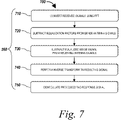
- FIG. 7 depicts a flow chart of an embodiment of a method of processing received tag response and noise-plus-interference signals.
- FIG. 8 depicts a flow chart of another embodiment of a method of processing received tag response and noise-plus-interference signals.
- an RFID tag reader system 100 includes one or more antenna elements 104 in communication with processing circuitry 108 .
- the antenna elements can be any type of an antenna element.
- the antenna elements 104 can be, but are not limited to, patch antennas, waveguide slot antennas, dipole antennas, and the like.
- Each antenna element of the RFID tag reader system 100 can be the same type of elements.
- the RFID tag reader system 100 incorporates two or more different types of antenna elements 104 .
- one or more of the antenna elements 104 includes a plurality of antenna elements (i.e., an array of antenna elements).
- the antenna elements 104 are multiplexed.
- an additional RFID tag reader system 100 ′ is mounted near a first RFID tag reader system 100 .
- one or more of the antenna elements 104 receives the response signals from RFID tags 112 that are placed on items of a pallet 114 .
- These response signals also include a noise component that is the result of the RF environment in which the RFID tag reader system 100 operates.
- the second tag reader system 100 ′ also can transmit signals, which can be received by a receiving antenna element 104 a .
- the signals transmitted from an antenna element 104 b ′ of the second tag reader system 100 ′ which is located at an adjacent position to the first tag reader system 100 (e.g., an adjacent warehouse loading dock door), are coupled into the receiving antenna 104 a of the reader under test 100 .
- the transmitted signals from the second reader 100 ′ may be on the order of +36 dBm effective isotropic radiated power (EIRP).
- These signals can have modulation and/or noise components according to a spectral mask (such as the EPC Global Class 1 Generation 2 Annex G Dense Interrogator Mode spectral mask) on the order of ⁇ 29 dBm EIRP within the tag signal response band.
- a spectral mask such as the EPC Global Class 1 Generation 2 Annex G Dense Interrogator Mode spectral mask
- the response signal from an RFID tag 112 is on the order of ⁇ 80 dBm EIRP.
- the weak tag response signals are overpowered by the transmitted signals from the jammers.
- the noise and interference can take other forms.
- fluorescent lights can generate RF noise and interference, as when an incident reader signal is backscattered from the periodically ionized gases in the fluorescent light.
- the noise and interference can results from the backscattering noise produced by time varying reflection present in the environment.
- other wireless items operating in the environment of the RFID tag reader system 100 can generate noise, such as legacy wireless LAN equipment, cordless telephones, or other industrial, scientific, or medical (ISM) devices.
- ISM industrial, scientific, or medical
- one embodiment of the RFID tag reader system 100 includes a sense antenna 116 .
- the sense antenna 116 samples the local RF environment, primarily for the purpose of sampling the transmitted signals sent by “jammers” preferentially to tag response signals.
- the sense antenna may perform this preferential reception by means of an antenna radiation pattern that favors reception of the noise source(s) over reception of tag responses.
- This sampled energy is transferred to a “sense receiver” that is part of the processing circuitry 108 of the RFID tag reader 100 .
- the processing circuitry 108 uses the sampled noise information extracted from the signals received by the sense antenna 116 to effectively subtract the sampled noise from the signals received by the receiving antenna 104 a of the RFID tag reader 100 .
- this is accomplished using a noise rejection algorithm.
- a higher signal-to-noise ratio also referred to as signal-to-noise-plus-interference ratio throughout the specification
- PER packet error rate
- Lower packet error rate in turn translates into improved RFID system performance, by increasing the number of tags that can be successfully read within a certain amount of time or by increasing the reliability of the tag reading operation.
- the sense antenna 116 is a separate antenna element that is in communication with RFID tag reader system 100 .
- the sense antenna 116 can be collocated within the RFID tag reader system 100 .
- the sense antenna 116 is configured to sample the local RF environment and preferentially receive signals from jammers at a higher signal level than tag response signals.
- the received signals can include noise and interference signals from the second RFID tag reader system 100 ′ and other interference sources.
- the sense antenna 116 can take various forms.
- the sense antenna 116 may be an omnidirectional monopole antenna.
- the sense antenna 116 is separate from the other antenna elements 104 of the RFID tag reader system 100 .
- the sense antenna 116 can be, but is not limited to, patch antennas, waveguide slot antennas, dipole antennas, and the like. In essence, any type of antenna can be used as the sense antenna 116 .
- the sense antenna element 116 need not be collocated with the reader under test. Said another way, the use of spatial diversity (e.g., antenna position) or polarization diversity can be employed to preferentially couple more noise and interference into the sense antenna 116 than tag response signal.
- the sense antenna's radiation pattern can be configured to favor reception of noise and interference preferentially over tag responses.
- beam steering techniques in the case where the sense antenna 116 is an array or a mechanically steered antenna, can be used to preferentially receive the noise-plus-interference signal from the second RFID tag reader system 100 ′.
- the sense antenna 116 is one of the antenna elements 104 of the RFID tag reader system 100 that is not in use for the tag response signal reception task.
- the processing circuitry 108 can include circuitry and/or software that provides the ability to switch among the antenna elements 104 which antenna element 104 is dedicated to receiving (i.e., the sense antenna 116 ) the noise signals from the second RFID tag reader system 100 ′.
- the sense antenna 116 can be switchably connected to either dedicated noise reception circuitry or tag response reception circuitry. This can take the form of an antenna element 104 that is not selected by the reader's processing circuitry 108 but is instead selected for connection to the noise cancellation circuitry.
- the processing circuitry 108 of the RFID tag reader system 100 processes the received signals to increase the signal-to-noise ratio of the tag response.
- the analog portion 200 of the processing circuitry 108 includes main reader (also referred to as main receiver through the specification) circuitry 202 and sense receiver circuitry 204 .
- the main reader circuitry 200 includes various components such as an in-phase demodulator, a quadrature demodulator, one or more filters, and one or more amplifiers.
- One or more of the various components of the main reader circuitry 200 may communicate with the sense reader circuitry 204 .
- the sense receiver circuitry 204 includes at least some duplicate components of the main reader circuitry 200 .
- the sense receiver circuitry 204 includes duplicates of the in-phase demodulator, the quadrature demodulator, the one or more filters, and the one or more amplifiers.
- the sense receiver circuitry 204 is an additional quadrature demodulator that is a replica of the main reader circuitry 200 .
- the sense receiver circuitry 204 is driven from the same local oscillator as the main receiver circuitry 200 . As such, the sense receiver circuitry 204 is tuned to the same frequency as the main reader circuitry 200 . In another embodiment, the sense receiver circuitry 204 is driven from a separate local oscillator (not shown).
- the sense antenna 116 and the sense receiver circuitry 204 cooperate to sample the local RF environment in which the RFID tag reader system 100 operates.
- the main reader circuitry 200 generates one or more received analog response signals 208 (e.g., in-phase and quadrature signals). These signals are also referred to as response signals 208 throughout the specification.
- the sense receiver circuitry 204 generates one or more received analog interference signals 212 (e.g., in-phase and quadrature signals). These signals are also referred to as noise-plus-interference signals.
- the sense receiver circuitry 204 cooperates with a digital circuit 300 described below in connection with FIG. 3 to convert a desired bandwidth, which preferably includes the bandwidth of the tag responses, to a digitized baseband signal for further processing.
- the digitized sense receiver signal is used in cooperation with a digitized main reader circuitry signal to increase the signal-to-noise ratio of the tag responses.
- the digital portion 300 includes a main digital receiver section 302 and sense digital receiver section 304 .
- the main digital receiver section 302 includes an analog to digital converter 308 (RX ADC) in communication with to the main reader circuitry 202 of FIG. 2 that receives the analog response signals 208 from the main reader circuitry 202 .
- the RX ADC 308 is also communicates with a first-in-first-out (RX FIFO) memory 312 .
- RX FIFO first-in-first-out
- FIG. 3 one embodiment of the digital portion 300 of the processing circuitry 108 is shown and described.
- the digital portion 300 includes a main digital receiver section 302 and sense digital receiver section 304 .
- the main digital receiver section 302 includes an analog to digital converter 308 (RX ADC) in communication with to the main reader circuitry 202 of FIG. 2 that receives the analog response signals 208 from the main reader circuitry 202 .
- the RX ADC 308 is also communicates with a first-in-first
- the sense digital receiver section 304 includes an analog to digital converter 316 (RX ADC) that communicates with the main reader circuitry 204 of FIG. 2 to receive the analog noise-plus-interference signals 212 from the main reader circuitry 204 .
- the RX ADC 316 is communicates with a first-in-first-out (FIFO) memory 320 .
- FIFO first-in-first-out
- FIG. 3 Although shown as having a single RX ADC 308 , it should be understood that additional RX ADCs 308 can be used. For example, each of the in-phase signal and quadrature signals can be fed into a respective RX ADC 308 .
- additional FIFO memories 320 can be used to store each of the respective digitized signals.
- the digitized signals are communicated to a digital signal processor (DSP) 324 .
- DSP digital signal processor
- the DSP periodically access the FIFO memories, retrieves the digitized signals, and processes the digital signals.
- One or more known noise rejection algorithms are applied to the digitized signals by the DSP 324 to increase the signal-to-noise ratio of the tag responses.
- an embodiment of a method 400 of increasing the signal-to-noise-plus-interference ration of an RFID tag response includes receiving (STEP 400 ) a radio frequency tag response, receiving (STEP 420 ) a noise-plus-interference signal, and processing (STEP 430 ) the received radio frequency tag response and the noise-plus-interference signal to increase the ratio between the two signals.
- the received tag responses and noise-plus-interference signals are equalized (STEP 424 , shown in phantom) before they are processed.
- one or more antenna elements 104 receives (STEP 410 ) the RFID tag response.
- the antenna element 104 receives (STEP 410 ) the tag response in the near field.
- the antenna element 104 receives (STEP 410 ) the tag response in the far field.
- the received tag responses are represented as a quadrature downconverted signal that is, in turn, digitized.
- the tag response signals are received (STEP 140 ) in near real-time after being irradiated by a tag reader system 100 transmission.
- the response signals are received (STEP 140 ) at some time after irradiation.
- some RFID tags can include capacitors that store the irritated energy, which can be used for processing if the RFID tag also includes a processing elements and subsequent transmission locally processed data to the receiving antennas 104 .
- the sense antenna 116 receives (STEP 420 ) the noise-plus-interference signal.
- a dedicated antenna element is added to the RFID tag reader system 100 and is configured to preferentially receive the noise-plus-interference signal that results from the operational environment.
- the sense antenna 116 is one of the antenna elements 104 that are not used to receive the tag response signals.
- the sense antenna receives (STEP 420 ) the noise-plus-interference signal in either the near field or the far field. The received noise-plus-interference is communicated to the dedicated noise-plus-interference reception circuitry for processing.
- the processing circuitry 108 processes (STEP 430 ) the received tag response signals and noise-plus-interference signals.
- the processing includes applying a noise cancellation algorithm to the received signals.
- noise cancellation algorithms can include, but are not limited to, a least mean square (LMS) algorithm or a recursive least squares (RLS) algorithm. These algorithms typically take the form of an adaptive weighting of a sampled noise-plus-interference signal which is subtracted from a received tag signal.
- the method 400 optionally includes equalizing (STEP 424 ) the received signals prior to processing the received signals.
- the equalization can be performed on a periodic basis or continually depending on the processing capabilities of the processing circuitry 108 .
- the equalization can be performed using at least one or more of the various techniques described below, although other techniques that are not described can also be used.
- the equalization (STEP 424 ) operation is performed to equalize the amplitude and phase response of the analog sense receiver circuitry 204 and digital sense receiver circuitry 304 with respect to the analog main reader circuitry 202 and digital main reader circuitry 302 .
- This operation is not continuously performed; instead it is periodically performed at an interval sufficient to compensate for changes in RF path lengths or antenna element 104 behavior caused by RFID tag reader system 100 component drift, mechanical changes to the RFID tag reader system 100 configuration, or due to the movement of reflective objects in the near and far fields of the RFID tag reader system 100 .
- the equalization process is performed at time intervals when the tags 112 are known not to be responding (e.g., during intervals when the transmitter of the reader under test is off).
- a method 500 of equalizing (STEP 424 ) the received signals includes identifying (STEP 510 ) the noise cancellation band, selecting (STEP 520 ) marker frequencies, and sampling (STEP 530 ) the main receiver and sense receiver signals.
- the method also includes converting (STEP 540 ) the sampled signals from the time domain to the frequency domain, calculating (STEP 550 ) equalization factors, and applying (STEP 560 ) the equalization factors to the received signals.
- a technician or end-user identifies (STEP 510 ) the desired noise cancellation band and configures the RFID tag reader system accordingly.
- This desired cancellation band may be chosen on the basis of a measurement of a noise and interference profile in a particular spatial region.
- the noise cancellation band may be selected to achieve cancellation of the noise or interference generated by a particular type of RFID reader or RFID reader waveform, or intermodulation distortion produced by nonlinearities causing mixing between two RFID reader signals. The nonlinear mixing may take place in an RFID reader's receiver circuitry or in another nonlinear element of the system.
- the noise cancellation band may be selected to cancel another source of noise or interference such as cellular telephone signals or intermodulation distortion caused by cellular telephone, paging, or mobile radio communication signals that would otherwise interfere with tag reading.
- the system may be configured by communicating system settings via a network connection from a central server to a network of readers, or manually by interaction with each reader's settings web page individually.
- the noise cancellation setup is done automatically and can be continuously changed and updated.
- the tag response subcarrier band for a particular RFID tag protocol or group of protocols is the desired noise cancellation band.
- this cancellation band is between about 200 kHz-300 kHz.
- the desired noise cancellation band is between about 18 kHz-100 kHz, which correspond to traditional fluorescent lights and ballasts excitation frequencies.
- the noise cancellation setup may be controlled by a scheduler that interleaves various operating modes (such as RFID tag protocol, operating frequency, data rates, modulation types, etc), so that the noise cancellation setup is chosen to automatically correspond to those settings offering improved performance for the selected operating mode.
- various operating modes such as RFID tag protocol, operating frequency, data rates, modulation types, etc
- the technician selects (STEP 520 ) one or more marker frequencies within the noise cancellation band.
- marker frequencies are selected from a table or dynamically computed to correspond to the desired operating mode. For example, four discrete frequencies that are equally spaced within the noise cancellation band can be used. In other examples, more or less frequencies can be used. Also, it should be understood that the frequencies need not be equally spaced.
- marker frequencies are chosen to be particularly closely spaced in frequency bands that contain more noise power, or frequency bands in which the reader's data demodulator is particularly sensitive to interference.
- the marker frequencies receive preferential noise cancellation so the marker frequencies may be chosen on that basis. The identified marker frequencies are used, as described below, to generate equalization coefficients for both amplitude and phase.
- the processing circuitry samples (STEP 530 ) both the main receiver signals and the sense receiver signals. In one embodiment, this sampling occurs simultaneously for a given interval of time. In other embodiments, the sampling occurs on an alternating basis between the receivers for a given interval of time. In one embodiment, 12,500 samples of 14 bit resolution are taken for the main receiver and sense receiver in-phase and quadrature channels at a sampling rate of 4 Msa/sec. In this embodiment, the sampling duration is 3.125 milliseconds. In other embodiments, different sampling rates, durations, and sampling resolutions can be used.
- the processing circuitry 108 converts (STEP 540 ) the signals from the time domain to the frequency domain.
- a complex valued fast Fourier transform FFT
- a discrete Fourier transform is used. It should be understood that other time domain to frequency domain conversions can be used, such as any of the family of Hadamard transforms or z-transforms.
- a wavelet method may also be used as part of a wavelet domain embodiment of the invention.
- the processing circuitry 108 calculates (STEP 550 ) an equalization factor for both phase and amplitude.
- an FFT response bin e.g., frequency
- the main receiver FFT shows a response magnitude of M 1 and a phase of Phi 1 .
- the sense receiver shows a response magnitude of M 2 and a phase of Phi 2 .
- the derivation of the equalization coefficients can also be performed in the time domain.
- the equalization may be performed by adjusting the equalization coefficients in order to minimize the mean square error between the desired output signal and the noisy input signal. In some embodiments, this adjustment is performed as a recursive process on a time series of tag response signals and sense receiver signals.
- the equalization factors are determined using an emission mask associated with the second RFID tag reader system.
- an emission mask 600 for the first RFID tag reader system 100 and an emission mask 600 ′ for the second RFID tag reader system 100 ′ are shown.
- a response signal from RFID tags is shown centered in the frequency band between the maxima of the two emission masks, although this depends on the RFID protocol, modulation type, and data rate being employed.
- the emission masks can be different.
- the emission masks are defined by a radio frequency identification protocol. In that embodiment, different radio frequency identification protocols may employ different modulation types or rates and therefore have different emission masks.
- the emission masks are measured over the air by sampling the incoming noise signal and performing a peak finding operation on that sampled signal.
- the marker frequencies or equalization factors are determined by selecting the frequency regions of the emission mask that contain the most energy in the desired tag response band.
- the equalization coefficients are determined using ratiometric comparisons of the response signals received by an antenna element 104 and the noise-plus-interference signals received by the sense antenna 116 .
- the ratiometric comparison is performed in the time domain.
- the ratiometric comparison is performed in the frequency domain.
- the equalization factors are determined in an effort to automatically match the magnitude and phase response of the main receiver and sense receiver systems. This can be advantageous when there are differences between the main receiver and sense receiver systems, such as when component tolerances in the two receivers result in different gain or phase responses.
- the sense receiver is deliberately designed to have reduced gain or unknown phase in order to minimize the cost or complexity of the sense receiver.
- the processing circuitry 108 applies (STEP 560 ) the equalization factors to the received response signals to increase the tag responses.
- one objective is to improve the signal-to-noise-plus-interference ratio for the received tag signals by subtracting some of the correlated noise (i.e., noise received by both in the main antenna 104 and sense antenna 116 ) while the tag returned power level is substantially unaltered.
- the equalization factors are used by a noise cancellation algorithm. As previously described, various noise cancellation algorithms can be used.
- the noise cancellation algorithm subtracts the equalized, sampled noise from the sampled response signals.
- processing circuitry applies (STEP 560 ) the equalization factors in the frequency domain.
- a method 700 of applying the equalization factors is described.
- the method includes converting (STEP 710 ) the received signals from both the sense antenna 116 and receiving antenna 104 , subtracting (STEP 720 ) the equalization factors from the transformed sense antenna signal, and subtracting (STEP 730 ) the equalized sense antenna signal from receiving antenna signal.
- the method 700 also includes performing (STEP 740 ) an inverse transform on the processed receiving antenna signal and demodulating (STEP 750 ) the processed receiving antenna signal.
- the processing circuitry 108 receives the incoming signals from the main receiving antenna 104 and sense antenna 116 and converts them to a digital form for which (STEP 710 ) their FFTs are taken continuously In other embodiments, other time-to-frequency domain conversion techniques can be used.
- the processing circuitry 108 subtracts (STEP 720 ) the equalization factors from each sense antenna bin.
- the subtraction is a performed by vector subtraction.
- the subtractions are actually performed by vector multiplication. The subtraction results in an equalized sense antenna data.
- the processing circuitry 108 subtracts (STEP 730 ) the equalized sense antenna data from the main antenna FFT bin.
- the subtraction is a performed by vector subtraction.
- the subtractions are actually performed by vector multiplication. The subtraction results in tag response data in which the noise components are substantially reduced.
- the processing circuitry 108 performs (STEP 740 ) an inverse-Fourier transform on the equalized response data. In other embodiments, other frequency-to-time domain transforms are used. The reverse transformation results in a time domain signal that includes the tag response.
- the processing circuitry 108 demodulates (STEP 750 ) the time domain signal using known demodulation techniques. This described method 700 becomes more processor intense as the number of marker frequency bins is increased due to the increased number of mathematical operations that must be performed.
- processing circuitry applies (STEP 560 ) the equalization factors in the time domain.
- a method 800 of applying the equalization factors is described.
- the method 800 includes averaging (STEP 810 ) the magnitude equalization factors, fitting (STEP 820 ) the phase equalization factors to a linear model, and applying (STEP 830 ) the resulting magnitude and phase correction to the received signals.
- the method also includes performing (STEP 840 ) sample subtraction and demodulating (STEP 850 ) the processed tag response signals.
- the processing circuitry 108 averages (STEP 810 ) the magnitude equalization factors using a moving average technique. In another embodiment, a weighted average is used. It should be understood that other averaging techniques can also be applied.
- the averaging (STEP 810 ) results in a gain calibration factor for the sense antenna 116 .
- the processing circuitry 108 fits (STEP 820 ) the phase equalization factors to a linear model and the slope of the line is used to determine the best sample cycle offset (e.g., correlation offset) between the sense antenna data and the main antenna data.
- the best sample cycle offset e.g., correlation offset
- Various known fit to linear model techniques can be used (e.g., the general linear model).
- a nonlinear model may also be employed at the expense of additional processor loading.
- the processing circuitry 108 applies (STEP 830 ) the resulting magnitude and phase corrections to the sense antenna data in the time domain. This can be done, for example, by multiplying each sense antenna data sample by the magnitude equalization factor and delaying the sense antenna dataset by the correlation offset. The application of the correction data results in an equalized sense data set.
- the processing circuitry 108 performs (STEP 840 ) sample subtraction. That is, the equalized sense data set is subtracted from the received tag response signal data.
- the processing circuitry 108 demodulates (STEP 850 ) the resultant data set P 1 . . . P n .
- the samples are communicated to a tag signal demodulation algorithm. It should be understood that various demodulation algorithms can be used.
Abstract
Description
Claims (38)
Priority Applications (1)
| Application Number | Priority Date | Filing Date | Title |
|---|---|---|---|
| US11/422,075 US7706764B2 (en) | 2006-06-03 | 2006-06-03 | Systems and methods for active noise cancellation in an RFID tag reader |
Applications Claiming Priority (1)
| Application Number | Priority Date | Filing Date | Title |
|---|---|---|---|
| US11/422,075 US7706764B2 (en) | 2006-06-03 | 2006-06-03 | Systems and methods for active noise cancellation in an RFID tag reader |
Publications (2)
| Publication Number | Publication Date |
|---|---|
| US20070280369A1 US20070280369A1 (en) | 2007-12-06 |
| US7706764B2 true US7706764B2 (en) | 2010-04-27 |
Family
ID=38790154
Family Applications (1)
| Application Number | Title | Priority Date | Filing Date |
|---|---|---|---|
| US11/422,075 Expired - Fee Related US7706764B2 (en) | 2006-06-03 | 2006-06-03 | Systems and methods for active noise cancellation in an RFID tag reader |
Country Status (1)
| Country | Link |
|---|---|
| US (1) | US7706764B2 (en) |
Cited By (5)
| Publication number | Priority date | Publication date | Assignee | Title |
|---|---|---|---|---|
| US20100120368A1 (en) * | 2008-11-13 | 2010-05-13 | John Stephen Smith | Noise cancellation for rfid backscatter |
| US20110221633A1 (en) * | 2010-03-11 | 2011-09-15 | Benjamin Bela Schramm | Methods and systems for determining the distance between two objects using wirelessly transmitted pulses |
| US20150144694A1 (en) * | 2013-11-26 | 2015-05-28 | Electronics And Telecommunications Research Institute | Loop antenna and method for switching the same |
| CN110445556A (en) * | 2019-07-30 | 2019-11-12 | 成都安杰联科技有限公司 | A kind of device and method of detection and positioning ETC interference unit |
| US11308462B2 (en) | 2014-05-13 | 2022-04-19 | Clear Token Inc | Secure electronic payment |
Families Citing this family (8)
| Publication number | Priority date | Publication date | Assignee | Title |
|---|---|---|---|---|
| US7693493B2 (en) * | 2007-06-29 | 2010-04-06 | Intel Corporation | Reducing amplitude modulated noise for a wireless transceiver |
| US8279112B2 (en) * | 2008-11-03 | 2012-10-02 | Trimble Navigation Limited | Methods and apparatuses for RFID tag range determination |
| KR101536696B1 (en) * | 2009-02-02 | 2015-07-14 | 삼성전자주식회사 | RFID(Radio Frequency IDentification) Interrogator |
| DE102009057349B4 (en) * | 2009-12-07 | 2014-03-20 | Nofilis Autoid Gmbh | Method and device for differentiating between useful signals and interfering signals in RFID tags |
| US8719930B2 (en) * | 2010-10-12 | 2014-05-06 | Sonus Networks, Inc. | Real-time network attack detection and mitigation infrastructure |
| DE102011103213B4 (en) * | 2011-06-01 | 2014-09-11 | Nofilis Autoid Gmbh | Method and detection device for differentiating signals of moving and stationary signal transmitters |
| CN105466549B (en) * | 2015-11-18 | 2018-06-05 | 中国科学院新疆天文台 | A kind of control system in radio astronomy receiver noise source |
| CN110830128B (en) * | 2018-08-07 | 2022-03-08 | 航天信息股份有限公司 | Signal receiving sensitivity detection system and method |
Citations (38)
| Publication number | Priority date | Publication date | Assignee | Title |
|---|---|---|---|---|
| US4210910A (en) | 1979-01-15 | 1980-07-01 | Calspan Corporation | Decoder for a space retrodirective array |
| US4924210A (en) | 1987-03-17 | 1990-05-08 | Omron Tateisi Electronics Company | Method of controlling communication in an ID system |
| US5425032A (en) | 1992-04-07 | 1995-06-13 | Hughes Aircraft Company | TDMA network and protocol for reader-transponder communications and method |
| US5537398A (en) | 1995-05-12 | 1996-07-16 | Motorola, Inc. | Apparatus for multi-rate simulcast communications |
| US5604486A (en) | 1993-05-27 | 1997-02-18 | Motorola, Inc. | RF tagging system with multiple decoding modalities |
| WO1999034526A1 (en) | 1997-12-24 | 1999-07-08 | Parakan Pty. Ltd. | A transmitter and a method for transmitting data |
| US5990820A (en) | 1996-05-07 | 1999-11-23 | Telefonaktiebolaget Lm Ericsson | Current-mode pipelined ADC with time-interleaved sampling and mixed reference and residue scaling |
| US6122329A (en) | 1998-02-06 | 2000-09-19 | Intermec Ip Corp. | Radio frequency identification interrogator signal processing system for reading moving transponders |
| US6172609B1 (en) | 1997-05-14 | 2001-01-09 | Avid Identification Systems, Inc. | Reader for RFID system |
| US6334051B1 (en) * | 1998-03-04 | 2001-12-25 | Kabushiki Kaisha Toshiba | Direct conversion receiver with wide band analog frequency conversion front end and digital demodulating and selecting back end |
| US20020079741A1 (en) | 2000-12-22 | 2002-06-27 | Anderson William J. | Automatic transfer switch and engine control |
| US20020154653A1 (en) | 2001-01-02 | 2002-10-24 | Mathilde Benveniste | Random medium access methods with backoff adaptation to traffic |
| US6492933B1 (en) | 1999-09-02 | 2002-12-10 | Mcewan Technologies, Llc | SSB pulse Doppler sensor and active reflector system |
| US6509828B2 (en) | 1998-07-30 | 2003-01-21 | Prc Inc. | Interrogating tags on multiple frequencies and synchronizing databases using transferable agents |
| US6529488B1 (en) | 1998-08-18 | 2003-03-04 | Motorola, Inc. | Multiple frequency allocation radio frequency device and method |
| US6563417B1 (en) | 1998-10-26 | 2003-05-13 | Identec Solutions Inc. | Interrogation, monitoring and data exchange using RFID tags |
| US20030104848A1 (en) * | 2001-11-30 | 2003-06-05 | Raj Brideglall | RFID device, system and method of operation including a hybrid backscatter-based RFID tag protocol compatible with RFID, bluetooth and/or IEEE 802.11x infrastructure |
| US6617962B1 (en) | 2000-01-06 | 2003-09-09 | Samsys Technologies Inc. | System for multi-standard RFID tags |
| US6631170B1 (en) * | 1999-12-03 | 2003-10-07 | Nokia Corporation | Radio frequency receiver |
| US20030214389A1 (en) | 2002-04-01 | 2003-11-20 | Matrics, Inc. | Method and system for optimizing an interrogation of a tag population |
| US6674327B2 (en) | 2002-04-02 | 2004-01-06 | Northrop Grumman Corporation | Combined multiplexer and switched gain circuit |
| US20040022204A1 (en) | 2002-07-31 | 2004-02-05 | Matthew Trembley | Full duplex/half duplex serial data bus adapter |
| US6735426B1 (en) | 2001-01-25 | 2004-05-11 | National Semiconductor Corporation | Multiple-band wireless transceiver with quadrature conversion transmitter and receiver circuits |
| US20040190092A1 (en) | 1999-09-17 | 2004-09-30 | Kia Silverbrook | Scanning device for coded data |
| US6812824B1 (en) | 1996-10-17 | 2004-11-02 | Rf Technologies, Inc. | Method and apparatus combining a tracking system and a wireless communication system |
| US20040222878A1 (en) | 2003-05-06 | 2004-11-11 | Ari Juels | Low-complexity cryptographic techniques for use with radio frequency identification devices |
| US20050035849A1 (en) | 2003-08-12 | 2005-02-17 | Yadgar Yizhack | Method and system for inventory count of articles with RFID tags |
| US20050286660A1 (en) | 2004-06-28 | 2005-12-29 | X-Cyte, Inc., A California Corporation | Digital frequency determining apparatus using matched filters |
| US20060023813A1 (en) | 2004-07-30 | 2006-02-02 | Broadcom Corporation | Apparatus and method for integration of tuner functions in a digital receiver |
| US20060022815A1 (en) * | 2004-07-30 | 2006-02-02 | Fischer Jeffrey H | Interference monitoring in an RFID system |
| US7002505B2 (en) | 2002-07-20 | 2006-02-21 | Koninklijke Philips Electronics N.V. | Switched-current analogue-to-digital converter |
| US7075412B1 (en) | 2002-05-30 | 2006-07-11 | Thingmagic L.L.C. | Methods and apparatus for operating a radio device |
| US20060186995A1 (en) * | 2005-02-22 | 2006-08-24 | Jiangfeng Wu | Multi-protocol radio frequency identification reader tranceiver |
| WO2006093984A2 (en) | 2005-02-28 | 2006-09-08 | Sirit Technologies Inc. | High-efficiency rf amplifier and envelope modulator |
| US7119736B2 (en) * | 2001-11-09 | 2006-10-10 | Siemens Aktiengesellschaft | Transponder system and method for measurement of separation |
| US7227449B2 (en) | 1999-06-10 | 2007-06-05 | Cubic Corporation | Multiple protocol smart card communication device |
| US7327775B1 (en) * | 1999-12-23 | 2008-02-05 | Nokia Corporation | CDMA receiver |
| US7383025B2 (en) * | 2001-01-12 | 2008-06-03 | Yongnan Xuan | Method for processing RF signals for receiving and transmission |
-
2006
- 2006-06-03 US US11/422,075 patent/US7706764B2/en not_active Expired - Fee Related
Patent Citations (39)
| Publication number | Priority date | Publication date | Assignee | Title |
|---|---|---|---|---|
| US4210910A (en) | 1979-01-15 | 1980-07-01 | Calspan Corporation | Decoder for a space retrodirective array |
| US4924210A (en) | 1987-03-17 | 1990-05-08 | Omron Tateisi Electronics Company | Method of controlling communication in an ID system |
| US5425032A (en) | 1992-04-07 | 1995-06-13 | Hughes Aircraft Company | TDMA network and protocol for reader-transponder communications and method |
| US5604486A (en) | 1993-05-27 | 1997-02-18 | Motorola, Inc. | RF tagging system with multiple decoding modalities |
| US5537398A (en) | 1995-05-12 | 1996-07-16 | Motorola, Inc. | Apparatus for multi-rate simulcast communications |
| US5990820A (en) | 1996-05-07 | 1999-11-23 | Telefonaktiebolaget Lm Ericsson | Current-mode pipelined ADC with time-interleaved sampling and mixed reference and residue scaling |
| US6812824B1 (en) | 1996-10-17 | 2004-11-02 | Rf Technologies, Inc. | Method and apparatus combining a tracking system and a wireless communication system |
| US6172609B1 (en) | 1997-05-14 | 2001-01-09 | Avid Identification Systems, Inc. | Reader for RFID system |
| WO1999034526A1 (en) | 1997-12-24 | 1999-07-08 | Parakan Pty. Ltd. | A transmitter and a method for transmitting data |
| US6122329A (en) | 1998-02-06 | 2000-09-19 | Intermec Ip Corp. | Radio frequency identification interrogator signal processing system for reading moving transponders |
| US6334051B1 (en) * | 1998-03-04 | 2001-12-25 | Kabushiki Kaisha Toshiba | Direct conversion receiver with wide band analog frequency conversion front end and digital demodulating and selecting back end |
| US6509828B2 (en) | 1998-07-30 | 2003-01-21 | Prc Inc. | Interrogating tags on multiple frequencies and synchronizing databases using transferable agents |
| US6529488B1 (en) | 1998-08-18 | 2003-03-04 | Motorola, Inc. | Multiple frequency allocation radio frequency device and method |
| US6563417B1 (en) | 1998-10-26 | 2003-05-13 | Identec Solutions Inc. | Interrogation, monitoring and data exchange using RFID tags |
| US7227449B2 (en) | 1999-06-10 | 2007-06-05 | Cubic Corporation | Multiple protocol smart card communication device |
| US6492933B1 (en) | 1999-09-02 | 2002-12-10 | Mcewan Technologies, Llc | SSB pulse Doppler sensor and active reflector system |
| US20040190092A1 (en) | 1999-09-17 | 2004-09-30 | Kia Silverbrook | Scanning device for coded data |
| US6631170B1 (en) * | 1999-12-03 | 2003-10-07 | Nokia Corporation | Radio frequency receiver |
| US7327775B1 (en) * | 1999-12-23 | 2008-02-05 | Nokia Corporation | CDMA receiver |
| US6617962B1 (en) | 2000-01-06 | 2003-09-09 | Samsys Technologies Inc. | System for multi-standard RFID tags |
| US20020079741A1 (en) | 2000-12-22 | 2002-06-27 | Anderson William J. | Automatic transfer switch and engine control |
| US20020154653A1 (en) | 2001-01-02 | 2002-10-24 | Mathilde Benveniste | Random medium access methods with backoff adaptation to traffic |
| US7383025B2 (en) * | 2001-01-12 | 2008-06-03 | Yongnan Xuan | Method for processing RF signals for receiving and transmission |
| US6735426B1 (en) | 2001-01-25 | 2004-05-11 | National Semiconductor Corporation | Multiple-band wireless transceiver with quadrature conversion transmitter and receiver circuits |
| US7119736B2 (en) * | 2001-11-09 | 2006-10-10 | Siemens Aktiengesellschaft | Transponder system and method for measurement of separation |
| US7215976B2 (en) * | 2001-11-30 | 2007-05-08 | Symbol Technologies, Inc. | RFID device, system and method of operation including a hybrid backscatter-based RFID tag protocol compatible with RFID, bluetooth and/or IEEE 802.11x infrastructure |
| US20030104848A1 (en) * | 2001-11-30 | 2003-06-05 | Raj Brideglall | RFID device, system and method of operation including a hybrid backscatter-based RFID tag protocol compatible with RFID, bluetooth and/or IEEE 802.11x infrastructure |
| US20030214389A1 (en) | 2002-04-01 | 2003-11-20 | Matrics, Inc. | Method and system for optimizing an interrogation of a tag population |
| US6674327B2 (en) | 2002-04-02 | 2004-01-06 | Northrop Grumman Corporation | Combined multiplexer and switched gain circuit |
| US7075412B1 (en) | 2002-05-30 | 2006-07-11 | Thingmagic L.L.C. | Methods and apparatus for operating a radio device |
| US7002505B2 (en) | 2002-07-20 | 2006-02-21 | Koninklijke Philips Electronics N.V. | Switched-current analogue-to-digital converter |
| US20040022204A1 (en) | 2002-07-31 | 2004-02-05 | Matthew Trembley | Full duplex/half duplex serial data bus adapter |
| US20040222878A1 (en) | 2003-05-06 | 2004-11-11 | Ari Juels | Low-complexity cryptographic techniques for use with radio frequency identification devices |
| US20050035849A1 (en) | 2003-08-12 | 2005-02-17 | Yadgar Yizhack | Method and system for inventory count of articles with RFID tags |
| US20050286660A1 (en) | 2004-06-28 | 2005-12-29 | X-Cyte, Inc., A California Corporation | Digital frequency determining apparatus using matched filters |
| US20060023813A1 (en) | 2004-07-30 | 2006-02-02 | Broadcom Corporation | Apparatus and method for integration of tuner functions in a digital receiver |
| US20060022815A1 (en) * | 2004-07-30 | 2006-02-02 | Fischer Jeffrey H | Interference monitoring in an RFID system |
| US20060186995A1 (en) * | 2005-02-22 | 2006-08-24 | Jiangfeng Wu | Multi-protocol radio frequency identification reader tranceiver |
| WO2006093984A2 (en) | 2005-02-28 | 2006-09-08 | Sirit Technologies Inc. | High-efficiency rf amplifier and envelope modulator |
Non-Patent Citations (17)
| Title |
|---|
| EPC Radio Frequency Identity Protocols, Class-1 Generation-2 UHF RFID, Conformance Requirements, Version 1.0.2. Feb. 2005, 40 pages. |
| International Preliminary Report on Patentability, PCT/US2006/023180, mailed on Jan. 17, 2008. |
| International Search Report from PCT/US2007/084487, mailed Sep. 3, 2008. |
| International Search Report, PCT/US2006/023180, mailed on May 15, 2007. |
| International Search Report, PCT/US2008/051861, mailed on Dec. 23, 2008. |
| Juels, A. "RFID Security and Privacy: A Research Survey" XP002375728 Retrieved from the Internet Sep. 28, 2005. |
| Kwak, J. et al., "RFID System with Fairness Within the Framework of Security and Privacy" XP019026267, vol. 3813, Jan. 1, 2005. |
| THG-002 Office Action dated Aug. 17, 2009. |
| THG-002 Office Action dated Aug. 20, 2008. |
| THG-002 Office Action dated Feb. 5, 2009. |
| THG-002 Office Action dated Mar. 19, 2008. |
| THG-004 Restriction Requirement dated Jun. 8, 2009. |
| THG-019 Office Action dated Oct. 31, 2005. |
| THG-019: Notice of allowance for U.S. Appl. No. 10/448,053 dated Mar. 14, 2006. |
| Written Opinion of the International Searching Authority from PCT/US2007/084487 mailed Sep. 3, 2008. |
| Written Opinion of the International Searching Authority, PCT/US08/51861, mailed on Dec. 23, 2008. |
| Written Opinion of the International Searching Authority, PCT/US2006/023180, mailed on May 15, 2007. |
Cited By (8)
| Publication number | Priority date | Publication date | Assignee | Title |
|---|---|---|---|---|
| US20100120368A1 (en) * | 2008-11-13 | 2010-05-13 | John Stephen Smith | Noise cancellation for rfid backscatter |
| US8340581B2 (en) * | 2008-11-13 | 2012-12-25 | Alien Technology Corporation | Noise cancellation for RFID backscatter |
| US20110221633A1 (en) * | 2010-03-11 | 2011-09-15 | Benjamin Bela Schramm | Methods and systems for determining the distance between two objects using wirelessly transmitted pulses |
| US20150144694A1 (en) * | 2013-11-26 | 2015-05-28 | Electronics And Telecommunications Research Institute | Loop antenna and method for switching the same |
| US11308462B2 (en) | 2014-05-13 | 2022-04-19 | Clear Token Inc | Secure electronic payment |
| US11861572B2 (en) | 2014-05-13 | 2024-01-02 | Clear Token Inc. | Secure electronic payment |
| CN110445556A (en) * | 2019-07-30 | 2019-11-12 | 成都安杰联科技有限公司 | A kind of device and method of detection and positioning ETC interference unit |
| CN110445556B (en) * | 2019-07-30 | 2022-03-22 | 成都安杰联科技有限公司 | Device and method for detecting and positioning ETC (electronic toll Collection) interference unit |
Also Published As
| Publication number | Publication date |
|---|---|
| US20070280369A1 (en) | 2007-12-06 |
Similar Documents
| Publication | Publication Date | Title |
|---|---|---|
| US7706764B2 (en) | Systems and methods for active noise cancellation in an RFID tag reader | |
| US6526264B2 (en) | Wideband multi-protocol wireless radio transceiver system | |
| US7043208B2 (en) | Method and apparatus to reduce interference in a communication device | |
| US6836673B1 (en) | Mitigating ghost signal interference in adaptive array systems | |
| US6968171B2 (en) | Adaptive noise reduction system for a wireless receiver | |
| EP2117114B1 (en) | Super regenerative (SR) apparatus having plurality of parallel SR amplifiers tuned to distinct frequencies | |
| US8036624B2 (en) | Off-line channel tuning amplitude slope matched filter architecture | |
| US8032103B2 (en) | Tuning amplitude slope matched filter architecture | |
| US7456747B2 (en) | Method and device for suppressing a transmitting signal in a receiver of an RFID write/read unit | |
| EP1344333B1 (en) | Method and apparatus for mitigating inter-channel interference in adaptive array systems | |
| WO2006065891A2 (en) | Transmit/receive compensation in smart antenna systems | |
| US8184751B2 (en) | Integrated interference cancellation system architecture with distortion correction | |
| US7295145B2 (en) | Selective-sampling receiver | |
| WO2023278652A1 (en) | Self-interference cancellation for rfid tag readers | |
| US20180062696A1 (en) | Communication device and cancellation method | |
| WO2006078314A2 (en) | Selective-sampling receiver | |
| US8494472B1 (en) | Reconfigurable chirp fourier transform based continuous convolution processor | |
| Lei et al. | A multichannel self-interference cancellation prototyping system | |
| CN114513228B (en) | L-band high-speed frequency hopping data link non-cooperative interference cancellation device and method | |
| Rogozhnikov et al. | Direct patch interference cancellation in passive multi-position radar system | |
| GB2334625A (en) | Calibrating antenna array | |
| KR20210010417A (en) | Electronic apparatus including transceiver for calibrating i/q imbalance in millimeter wave communication system and thereof operating method | |
| WO2008065427A2 (en) | Radio frequency identification location system | |
| AU2002211433A1 (en) | Method and apparatus for mitigating inter-channel interference in adaptive array systems |
Legal Events
| Date | Code | Title | Description |
|---|---|---|---|
| AS | Assignment |
Owner name: THINGMAGIC, INC., MASSACHUSETTS Free format text: ASSIGNMENT OF ASSIGNORS INTEREST;ASSIGNOR:REYNOLDS, MATTHEW S.;REEL/FRAME:018009/0589 Effective date: 20060612 Owner name: THINGMAGIC, INC.,MASSACHUSETTS Free format text: ASSIGNMENT OF ASSIGNORS INTEREST;ASSIGNOR:REYNOLDS, MATTHEW S.;REEL/FRAME:018009/0589 Effective date: 20060612 |
|
| FEPP | Fee payment procedure |
Free format text: PAYOR NUMBER ASSIGNED (ORIGINAL EVENT CODE: ASPN); ENTITY STATUS OF PATENT OWNER: LARGE ENTITY |
|
| AS | Assignment |
Owner name: SILICON VALLEY BANK, CALIFORNIA Free format text: SECURITY AGREEMENT;ASSIGNOR:THINGMAGIC, INC.;REEL/FRAME:023741/0480 Effective date: 20080417 Owner name: SILICON VALLEY BANK,CALIFORNIA Free format text: SECURITY AGREEMENT;ASSIGNOR:THINGMAGIC, INC.;REEL/FRAME:023741/0480 Effective date: 20080417 |
|
| STCF | Information on status: patent grant |
Free format text: PATENTED CASE |
|
| AS | Assignment |
Owner name: THINGMAGIC INC,MASSACHUSETTS Free format text: RELEASE;ASSIGNOR:SILICON VALLEY BANK;REEL/FRAME:024402/0562 Effective date: 20100506 Owner name: THINGMAGIC INC, MASSACHUSETTS Free format text: RELEASE;ASSIGNOR:SILICON VALLEY BANK;REEL/FRAME:024402/0562 Effective date: 20100506 |
|
| FEPP | Fee payment procedure |
Free format text: PAYOR NUMBER ASSIGNED (ORIGINAL EVENT CODE: ASPN); ENTITY STATUS OF PATENT OWNER: LARGE ENTITY Free format text: PAYER NUMBER DE-ASSIGNED (ORIGINAL EVENT CODE: RMPN); ENTITY STATUS OF PATENT OWNER: LARGE ENTITY |
|
| AS | Assignment |
Owner name: TRIMBLE NAVIGATION LIMITED, CALIFORNIA Free format text: ASSIGNMENT OF ASSIGNORS INTEREST;ASSIGNOR:THINGMAGIC, INC.;REEL/FRAME:025644/0509 Effective date: 20101022 |
|
| FPAY | Fee payment |
Year of fee payment: 4 |
|
| AS | Assignment |
Owner name: TRIMBLE INC., CALIFORNIA Free format text: MERGER;ASSIGNOR:TRIMBLE NAVIGATION LIMITED;REEL/FRAME:040754/0633 Effective date: 20160930 |
|
| AS | Assignment |
Owner name: NOVANTA CORPORATION, MASSACHUSETTS Free format text: ASSIGNMENT OF ASSIGNORS INTEREST;ASSIGNOR:TRIMBLE INC.;REEL/FRAME:041262/0307 Effective date: 20170110 |
|
| AS | Assignment |
Owner name: BANK OF AMERICA, N.A., NORTH CAROLINA Free format text: SECURITY INTEREST;ASSIGNOR:NOVANTA CORPORATION;REEL/FRAME:041814/0920 Effective date: 20170331 |
|
| MAFP | Maintenance fee payment |
Free format text: PAYMENT OF MAINTENANCE FEE, 8TH YEAR, LARGE ENTITY (ORIGINAL EVENT CODE: M1552) Year of fee payment: 8 |
|
| FEPP | Fee payment procedure |
Free format text: MAINTENANCE FEE REMINDER MAILED (ORIGINAL EVENT CODE: REM.); ENTITY STATUS OF PATENT OWNER: LARGE ENTITY |
|
| LAPS | Lapse for failure to pay maintenance fees |
Free format text: PATENT EXPIRED FOR FAILURE TO PAY MAINTENANCE FEES (ORIGINAL EVENT CODE: EXP.); ENTITY STATUS OF PATENT OWNER: LARGE ENTITY |
|
| STCH | Information on status: patent discontinuation |
Free format text: PATENT EXPIRED DUE TO NONPAYMENT OF MAINTENANCE FEES UNDER 37 CFR 1.362 |
|
| FP | Lapsed due to failure to pay maintenance fee |
Effective date: 20220427 |