US7505744B1 - DC offset correction using multiple configurable feedback loops - Google Patents
DC offset correction using multiple configurable feedback loops Download PDFInfo
- Publication number
- US7505744B1 US7505744B1 US11/191,840 US19184005A US7505744B1 US 7505744 B1 US7505744 B1 US 7505744B1 US 19184005 A US19184005 A US 19184005A US 7505744 B1 US7505744 B1 US 7505744B1
- Authority
- US
- United States
- Prior art keywords
- signal
- configurable
- offset correction
- feedback loop
- digital
- Prior art date
- Legal status (The legal status is an assumption and is not a legal conclusion. Google has not performed a legal analysis and makes no representation as to the accuracy of the status listed.)
- Active, expires
Links
Images


Classifications
-
- H—ELECTRICITY
- H04—ELECTRIC COMMUNICATION TECHNIQUE
- H04B—TRANSMISSION
- H04B1/00—Details of transmission systems, not covered by a single one of groups H04B3/00 - H04B13/00; Details of transmission systems not characterised by the medium used for transmission
- H04B1/06—Receivers
- H04B1/16—Circuits
- H04B1/30—Circuits for homodyne or synchrodyne receivers
-
- H—ELECTRICITY
- H04—ELECTRIC COMMUNICATION TECHNIQUE
- H04L—TRANSMISSION OF DIGITAL INFORMATION, e.g. TELEGRAPHIC COMMUNICATION
- H04L25/00—Baseband systems
- H04L25/02—Details ; arrangements for supplying electrical power along data transmission lines
- H04L25/06—Dc level restoring means; Bias distortion correction ; Decision circuits providing symbol by symbol detection
- H04L25/061—Dc level restoring means; Bias distortion correction ; Decision circuits providing symbol by symbol detection providing hard decisions only; arrangements for tracking or suppressing unwanted low frequency components, e.g. removal of dc offset
Definitions
- the present invention relates to a wireless communication system, and more particularly to DC offset correction using multiple configurable feedback loops and performed during “training time” having no DC content.
- a common problem in wireless communication receivers is DC offset. This is especially a concern in Direct Conversion Receivers (DCRs) where received radio frequency (RF) signals are converted directly to baseband using a local oscillator (LO) signal having a frequency equal to the frequency of the received RF signals.
- DCRs Direct Conversion Receivers
- LO local oscillator
- the LO signal leaks to the inputs of mixers used to downconvert the RF signals, thereby creating a DC offset error associated with downconversion. Accordingly, there remains a need for a DC offset correction system that corrects DC offset errors caused by LO leakage as well as any other DC offsets in a receiver for a wireless communication system.
- the present invention provides a DC offset correction system for a wireless communication device that removes a DC offset from a baseband receive signal during “training time” when the baseband receive signal should ideally have no DC content.
- the DC offset correction system includes multiple configurable feedback loops that operate to remove, or cancel, the DC offset from the baseband receive signal.
- One or more of the multiple configurable feedback loops is activated, or set to a tracking mode of operation, for a period of time during reception when it is known that the received signal should ideally contain no DC content.
- This training time varies depending on the particular communication standard being used by the wireless communication device.
- one or more of the multiple configurable feedback loops may be set to a tracking mode during reception of the preamble and header of an IEEE 802.11 packet when the baseband receive signal should ideally have no DC content.
- the DC offset correction system is configured to have a DC notch filter transfer function.
- the DC offset correction system removes the DC offset and does not interfere with the reception of information contained in the baseband receive signal at a frequency above the cut-off frequency defined by the transfer function of the DC offset correction system.
- the multiple configurable feedback loops are deactivated, or set to a hold mode of operation, such that a DC offset correction provided by the DC offset correction system is held constant.
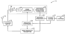
- FIG. 1 illustrates an exemplary embodiment of a mobile terminal including DC offset correction circuitry of the present invention
- FIG. 2 illustrates an exemplary embodiment of the DC offset correction circuitry of the present invention.
- the present invention is particularly well-suited for use in a mobile terminal, and particularly a mobile terminal that operates according to the IEEE 802.11 standard
- the present invention may be used in any wireless receiver operating according to a standard such as, but not limited to, the Global System for Mobile Communications (GSM) standard, the Time Division Multiple Access (TDMA) standard, the Code Division Multiple Access (CDMA) standard, the Wideband CDMA (WCDMA) standard, or the like, wherein the standard may define a “training time” during which received signals should have no DC content when downconverted to baseband.
- GSM Global System for Mobile Communications
- TDMA Time Division Multiple Access
- CDMA Code Division Multiple Access
- WCDMA Wideband CDMA
- the present invention is preferably incorporated in a mobile terminal 10 , such as a mobile telephone, personal digital assistant, Wireless Local Area Network (WLAN) device, or the like.
- the basic architecture of a mobile terminal 10 is represented in FIG. 1 , and may include a receiver front end 12 , a radio frequency transmitter 14 , an antenna 16 , a duplexer or switch 18 , a baseband processor 20 , a control system 22 , a frequency synthesizer 24 , and an interface 26 .
- the receiver front end 12 receives information-bearing radio frequency signals from one or more remote transmitters (not shown).
- a low noise amplifier (LNA) 28 amplifies the received signal.
- LNA low noise amplifier
- a filter circuit 30 minimizes broadband interference in the received signal, while downconversion circuitry 32 downconverts the filtered, received signal to a baseband signal.
- the baseband signal is then digitized and DC offset correction is performed by digitization and DC offset correction circuitry 34 .
- the receiver front end 12 typically uses one or more mixing frequencies generated by the frequency synthesizer 24 .
- the baseband processor 20 processes the digitized, received signal to extract the information or data bits conveyed in the received signal. This processing typically comprises demodulation, decoding, and error correction operations. As such, the baseband processor 20 is generally implemented in an Application Specific Interacted Circuit (ASIC) or one or more digital signal processors (DSPs).
- ASIC Application Specific Interacted Circuit
- DSPs digital signal processors
- the baseband processor 20 receives digitized data from the control system 22 , which it modulates for transmission.
- the control system 22 may run software stored in memory. Alternatively, the operation of the control system 22 may be a function of sequential logic structures as is well understood.
- the baseband processor 20 After modulating the data from the control system 22 , the baseband processor 20 outputs the modulated data to the radio frequency transmitter 14 .
- the radio frequency transmitter 14 operates to convert the modulated data into a radio frequency transmit signal at the desired output power level for transmission via antenna.
- a user may interact with the mobile terminal 10 via the interface 26 .
- the interface 26 may include devices such as, but not limited to, a microphone, a speaker, a keypad, and/or a display. Additionally, it may include a voice encoder/decoder, in which case it may communicate directly with the baseband processor 20 .
- FIG. 2 illustrates the digitization and DC offset correction circuitry 34 according to one embodiment of the present invention.
- the digitization and DC offset correction circuitry 34 includes multiple configurable feedback loops that operate to remove or cancel the DC offset from the input signal (INPUT), which is the output of the downcoversion circuitry 32 ( FIG. 1 ).
- One or more of the multiple configurable feedback loops is activated, or configured to be in a tracking mode of operation, for a period of time during operation when it is known that the received signal should ideally contain no DC content. This training time varies depending on the particular communication standard being used by the mobile terminal 10 ( FIG. 1 ).
- one or more of the multiple configurable feedback loops may be activated during reception of the preamble and header of an IEEE 802.11 packet. During reception of the preamble and header of an IEEE 802.11 packet, the baseband signal provided by the downconversion circuitry 32 ( FIG. 1 ) should ideally have no DC content.
- one or more of the multiple configurable feedback loops is in tracking mode and operates to remove or cancel the DC offset from the input signal.
- the digitization and DC offset correction circuitry 34 has a DC notch filter transfer function when one or more of the multiple configurable feedback loops is in the tracking mode.
- the digitization and DC offset correction circuitry 34 does not interfere with the reception of a signal, such as the preamble and header of an IEEE 802.11 packet, at a frequency above the cut-off frequency defined by the transfer function of the digitization and DC offset correction circuitry 34 .
- the multiple configurable feedback loops of the digitization and DC offset correction circuitry 34 are deactivated, or configured to be in a hold mode of operation, such that a DC offset correction provided by the digitization and DC offset correction circuitry 34 is held constant.
- the digitization and DC offset correction circuitry 34 includes a configurable digital feedback loop 36 , a configurable analog feedback loop 38 , and an analog-to-digital (A/D) converter 40 .
- the configurable digital feedback loop 36 is more generally referred to herein as a configurable inner feedback loop
- the configurable analog feedback loop 38 is more generally referred to herein as a configurable outer feedback loop.
- the configurable digital feedback loop 36 is within the configurable analog feedback loop 38
- the configurable digital and analog feedback loops 36 and 38 are referred to as nested configurable feedback loops.
- the input signal (INPUT) which is the analog baseband signal output by the downconversion circuitry 32 ( FIG. 1 ), is provided to differencing, or subtraction, circuitry 42 .
- the differencing circuitry 42 operates to provide a corrected analog input signal based on removing or subtracting an analog DC offset correction signal from the input signal (INPUT).
- the analog DC offset correction signal is generated by the configurable analog feedback loop 38 to remove essentially all or a portion of a DC offset from the input signal (INPUT).
- the configurable analog feedback loop 38 may be in a tracking mode where the analog DC offset correction signal is adjusted to remove the DC offset or in a hold mode where the analog DC offset correction signal is held constant.
- the output of the differencing circuitry 42 which is referred to herein as a corrected analog input signal is provided to the A/D converter 40 .
- the A/D converter 40 digitizes the corrected analog input signal to provide a digitized signal.
- the digitized signal is scaled by scaling circuitry 44 having a predetermined, or optionally controllable, scaling factor (K).
- K scaling factor
- the scaled signal is provided from the scaling circuitry 44 to differencing circuitry 46 .
- the differencing circuitry 46 provides a corrected digital signal based on removing or subtracting a digital DC offset correction signal generated by the configurable digital feedback loop 36 from the output of the scaling circuitry 44 .
- the digital DC offset correction signal is generated by the configurable digital feedback loop 36 to remove essentially all or a portion of a DC offset from the input signal (INPUT).
- the configurable digital feedback loop 36 may be in a tracking mode where the digital DC offset correction signal is adjusted to remove the DC offset or in a hold mode where the digital DC offset correction signal is held constant.
- the corrected digital signal output by the differencing circuitry 46 is provided to scaling circuitry 48 having a predetermined, or optionally controllable, scaling factor of 1/K. It should be noted that scaling circuitries 44 and 48 are optional and thus are not necessary for the present invention.
- the output signal (OUTPUT) provided at the output of the scaling circuitry 48 which is the output of the digitization and DC offset correction circuitry 34 , is digital version of the input signal (INPUT) having been compensated to remove, or cancel, the DC offset of the receiver front end 12 ( FIG. 1 ).
- the configurable digital feedback loop 36 is essentially a low-pass filter that operates to low-pass filter the output of the differencing circuitry 46 to provide the digital offset correction signal, where the digital offset correction signal is proportional to the DC content of the output of the differencing circuitry 46 .
- the configurable digital feedback loop 36 includes digital accumulation circuitry formed by summation circuitry 50 and delay circuitry 52 , arranged as shown.
- the digital accumulation circuitry operates to low-pass filter the corrected digital signal provided by differencing circuitry 46 .
- the filtered signal is scaled by scaling circuitry 54 having a controllable scaling factor ( ⁇ ).
- the controllable scaling factor ( ⁇ ) of the scaling circuitry 54 may be controlled, for example, by control system 22 or baseband processor 20 .
- the configurable digital feedback loop 36 is enabled or disabled by controlling the scaling factor ( ⁇ ) of the scaling circuitry 54 , and set to either the tracking mode or hold mode by hold signal (HOLD_A).
- the scaling factor ( ⁇ ) of the scaling circuitry 54 may be set to zero to disable the configurable digital feedback loop 36 such that the digital DC offset correction signal provided to the differencing circuitry 46 is always zero.
- the scaling factor ( ⁇ ) of the scaling circuitry 54 may be set to a value such as 1/512 in order to enable the configurable digital feedback loop 36 .
- the scaling factor ( ⁇ ) also controls the sharpness of the cut-off transient of the low-pass filter formed by summation circuitry 50 and delay circuitry 52 .
- the hold signal (HOLD_A) is set to a first state to place the configurable digital feedback loop 36 in tracking mode where the output of the configurable digital feedback loop 36 is active.
- the configurable digital feedback loop 36 is placed in the tracking mode during training times when it is desirable to remove DC content from the input signal (INPUT).
- the hold signal (HOLD_A) is set to a second state to place the configurable digital feedback loop 36 in the hold mode such that the output of the delay circuitry 52 , and thus the digital DC offset correction signal provided to the differencing circuitry 46 , is held constant.
- the configurable analog feedback loop 38 is essentially a low-pass filter that operates to low-pass filter the output signal (OUTPUT) to provide the analog offset correction signal, where the analog offset correction signal is proportional to the DC content of the output signal (OUTPUT).
- the configurable analog feedback loop 38 includes digital accumulation circuitry formed by summation circuitry 56 and delay circuitry 58 , arranged as shown.
- the digital accumulation circuitry operates to low-pass filter the output signal (OUTPUT).
- the filtered signal from the delay circuitry 58 is scaled by scaling circuitry 60 having a controllable scaling factor ( ⁇ ).
- the controllable scaling factor ( ⁇ ) of the scaling circuitry 60 may be controlled, for example, by control system 22 or baseband processor 20 .
- the configurable analog feedback loop 38 is enabled or disabled by controlling the scaling factor ( ⁇ ) of the scaling circuitry 60 , and set to either the tracking mode or hold mode by hold signal (HOLD_B).
- the scaling factor ( ⁇ ) of the scaling circuitry 60 may be set to zero to disable the configurable analog feedback loop 38 such that the analog DC offset correction signal provided to the differencing circuitry 42 is always zero.
- the scaling factor ( ⁇ ) of the scaling circuitry 60 may be set to a value such as 1/512 in order to enable the configurable analog feedback loop 38 .
- the scaling factor ( ⁇ ) also controls the sharpness of the cut-off transient of the low-pass filter formed by summation circuitry 56 and delay circuitry 58 .
- the hold signal (HOLD_B) is set to a first state to place the configurable analog feedback loop 38 in an active mode.
- the configurable analog feedback loop 38 is placed in active mode during training times when it is desirable to remove DC content from the input signal (INPUT).
- the hold signal (HOLD_B) is set to a second state to place the configurable analog feedback loop 38 in an inactive state such that the output of the delay circuitry 58 , and thus the analog DC offset correction signal provided to the differencing circuitry 42 , is held constant.
- Limiting circuitry 62 operates to limit the input of digital-to-analog (D/A) converter 64 to a known maximum input value of the D/A converter. More specifically, the limiting circuitry 62 receives the output of the scaling circuitry 60 . If the output of the scaling circuitry 60 is less than or equal to the maximum input value of the D/A converter, then the scaling circuitry 60 simply passes the output of the scaling circuitry 60 to the input of the D/A converter 64 . However, if the output of the scaling circuitry 60 is greater than the maximum input value of the D/A converter 64 , the limiting circuitry 62 provides the maximum input value to the D/A converter 64 , thereby limiting the input of the D/A converter 64 to the known maximum input value.
- D/A digital-to-analog
- the transfer function of the digitization and DC offset correction circuitry 34 of FIG. 2 is:
- H ⁇ ( z ) 1 - z - 1 1 - ( 1 - ⁇ ) ⁇ z - 1 + ⁇ ⁇ ⁇ z - ( D + 1 ) , where D is a predetermined or selectable integer defining the delay of the D/A converter 64 .
- D is a predetermined or selectable integer defining the delay of the D/A converter 64 .
- the transfer function of the digitization and DC offset correction circuitry 34 is that of a DC notch filter. This is true whether one or both of the configurable digital feedback loop 36 and the configurable analog feedback loop 38 is enabled.
- the digitization and DC offset correction circuitry 34 operates to remove essentially all DC content from the input signal (INPUT). Frequencies other than DC pass through the digitization and DC offset correction circuitry 34 .
- the digitization and DC offset correction circuitry 34 operates to remove the DC content from the input signal (INPUT), thereby correcting the DC offset of the receiver front end 12 ( FIG. 1 ), without interfering with the reception of the preamble and header of the IEEE 802.11 packet.
- the configurable digital and analog feedback loops 36 and 38 are enabled and set to the tracking mode of operation during a training time. More specifically, the configurable digital feedback loop 36 may be enabled by setting the scaling factor ( ⁇ ) of the scaling circuitry 54 to a value other than zero, such as 1/512, and set to the tracking mode by providing the hold signal (HOLD_A) such that the output of the delay circuitry 52 is active, or not held constant.
- ⁇ scaling factor
- HOLD_A hold signal
- the configurable analog feedback loop 38 may be enabled by setting the scaling factor ( ⁇ ) of the scaling circuitry 60 to a value other than zero, such as 1/512, and set to the tracking mode by providing the hold signal (HOLD_B) such that the output of the delay circuitry 58 is active, or not held constant.
- the digital and/or analog DC offset correction signals are adjusted such that the DC offset is removed from the input signal (INPUT).
- the configurable digital and analog feedback loops 36 and 38 are set to the hold mode of operation such that the digital and analog DC offset correction signals are held constant. Thereafter, the digitization and DC offset correction circuitry 34 uses the constant values of the digital and analog DC offset correction signals to remove the DC offset from the input signal (INPUT).
- the configurable digital feedback loop 36 and the configurable analog feedback loop 38 may have different scales and resolutions.
- the configurable digital feedback loop 36 may have a large scale and coarse resolution, and the configurable analog feedback loop 38 may have a small scale and fine resolution.
- the configurable digital feedback loop 36 may have a scale of 30 mV (millivolts) with a resolution of 2 mV, and the configurable analog digital feedback loop 38 may have a scale of 3 mV with a resolution of 0.2 mV.
- the configurable digital and analog feedback loops 36 and 38 may have any desired scale and resolution.
- both the configurable digital and analog feedback loops 36 and 38 may initially be used to obtain initial values for the digital and analog DC offset correction signals. Thereafter, only the configurable analog feedback loop 38 may be periodically activated to readjust the analog DC offset correction signal to compensate for slight variations in the DC offset of the receiver front end 12 ( FIG. 1 ).
- the configurable digital feedback loop 36 may be activated if a variation in the DC offset of the receiver front end 12 ( FIG. 1 ) occurs that is large enough to move the DC offset outside the scale of the configurable analog feedback loop 38 . For example, if the scale of the configurable analog feedback loop 38 is 3 mV and the DC offset varies by an amount greater than 3 mV, the configurable digital feedback loop 36 may be activated.
- the digitization and DC offset correction circuitry 34 may operate in one of four modes of operation depending on the configuration of the configurable digital and analog feedback loops 36 and 38 .
- a digital mode the configurable digital feedback loop 36 is enabled, and the configurable analog feedback loop 38 is disabled.
- an analog mode the configurable analog feedback loop 38 is enabled, and the configurable digital feedback loop 36 is disabled.
- both the configurable digital feedback loop 36 and the configurable analog feedback loop 38 are enabled.
- a no-correction mode both the configurable digital feedback loop 36 and the configurable analog feedback loop 38 are disabled.
- the digitization and DC offset correction circuitry 34 of the present invention has substantial opportunity for variation without departing from the spirit or scope of the present invention.
- downconversion circuitry 32 FIG. 1
- the mobile terminal 10 may include first digitization and DC offset correction circuitry 34 to remove the DC offset from the in-phase component and second digitization and DC offset correction circuitry 34 to remove the DC offset from the quadrature component.
Abstract
Description
where D is a predetermined or selectable integer defining the delay of the D/A converter 64. As will be apparent to one of ordinary skill in the art, the transfer function of the digitization and DC offset
Claims (20)
Priority Applications (1)
| Application Number | Priority Date | Filing Date | Title |
|---|---|---|---|
| US11/191,840 US7505744B1 (en) | 2005-07-28 | 2005-07-28 | DC offset correction using multiple configurable feedback loops |
Applications Claiming Priority (1)
| Application Number | Priority Date | Filing Date | Title |
|---|---|---|---|
| US11/191,840 US7505744B1 (en) | 2005-07-28 | 2005-07-28 | DC offset correction using multiple configurable feedback loops |
Publications (1)
| Publication Number | Publication Date |
|---|---|
| US7505744B1 true US7505744B1 (en) | 2009-03-17 |
Family
ID=40434141
Family Applications (1)
| Application Number | Title | Priority Date | Filing Date |
|---|---|---|---|
| US11/191,840 Active 2026-09-14 US7505744B1 (en) | 2005-07-28 | 2005-07-28 | DC offset correction using multiple configurable feedback loops |
Country Status (1)
| Country | Link |
|---|---|
| US (1) | US7505744B1 (en) |
Cited By (6)
| Publication number | Priority date | Publication date | Assignee | Title |
|---|---|---|---|---|
| US20070270149A1 (en) * | 2006-05-19 | 2007-11-22 | Oki Electric Industry Co., Ltd. | Handover control between base stations in a multi-hop mobile communication network |
| US20100039158A1 (en) * | 2008-08-12 | 2010-02-18 | Fujitsu Limited | Offset correction device and method |
| US20110201284A1 (en) * | 2008-04-21 | 2011-08-18 | Freescale Semiconductor, Inc. | Dc offset calibration in a direct conversion receiver |
| US20110293292A1 (en) * | 2010-05-28 | 2011-12-01 | Huan-Shang Tsai | Mitigating Signal Offsets in Optical Receivers |
| CN101795251B (en) * | 2010-01-20 | 2012-11-21 | 华为技术有限公司 | Device and method for generation feedback signal |
| US20180054262A1 (en) * | 2015-03-09 | 2018-02-22 | Sony Corporation | Device and method for determining a dc component |
Citations (29)
| Publication number | Priority date | Publication date | Assignee | Title |
|---|---|---|---|---|
| US5459679A (en) | 1994-07-18 | 1995-10-17 | Quantum Corporation | Real-time DC offset control and associated method |
| US5566213A (en) * | 1995-03-09 | 1996-10-15 | Motorola, Inc. | Selective call receiving device with improved symbol decoding and automatic frequency control |
| US5584059A (en) | 1993-06-30 | 1996-12-10 | Motorola, Inc. | DC offset reduction in a zero-if transmitter |
| US6166668A (en) | 1999-06-01 | 2000-12-26 | Motorola, Inc. | Method and apparatus for providing DC offset correction and hold capability |
| US6225848B1 (en) | 1999-04-13 | 2001-05-01 | Motorola, Inc. | Method and apparatus for settling and maintaining a DC offset |
| US6317064B1 (en) | 2000-02-29 | 2001-11-13 | Motorola, Inc. | DC offset correction adaptable to multiple requirements |
| US6321073B1 (en) | 2000-01-31 | 2001-11-20 | Motorola, Inc. | Radiotelephone receiver and method with improved dynamic range and DC offset correction |
| US6459889B1 (en) * | 2000-02-29 | 2002-10-01 | Motorola, Inc. | DC offset correction loop for radio receiver |
| US20020151289A1 (en) * | 2001-03-05 | 2002-10-17 | Mahibur Rahman | DC offset correction scheme for wireless receivers |
| US6509777B2 (en) | 2001-01-23 | 2003-01-21 | Resonext Communications, Inc. | Method and apparatus for reducing DC offset |
| US20030133518A1 (en) | 2002-01-11 | 2003-07-17 | Rf Micro Devices | Estimation and correction of DC offset in the presence of frequency offset |
| US20030199264A1 (en) * | 2002-04-09 | 2003-10-23 | Christian Holenstein | Direct current offset cancellation for mobile station modems using direct conversion |
| US20030231054A1 (en) * | 2002-06-13 | 2003-12-18 | Rahul Magoon | Sequential DC offset correction for amplifier chain |
| US20040081256A1 (en) * | 2002-10-24 | 2004-04-29 | Hong Shi | DC offset correcting in a direct conversion or very low if receiver |
| US6816718B2 (en) | 2002-02-07 | 2004-11-09 | Rf Micro Devices, Inc. | DC offset correction using dummy amplifier |
| US20040229580A1 (en) * | 2003-05-15 | 2004-11-18 | Peir-Weir Chen | Direct conversion receiver with DC offset compensation and method thereof |
| US20050111525A1 (en) * | 2003-08-26 | 2005-05-26 | Bas Driesen | Method and apparatus for estimating DC offset in an orthogonal frequency division multiplexing system |
| US6903606B1 (en) | 2003-08-25 | 2005-06-07 | Rf Micro Devices, Inc. | DC offset correction using unused LNA |
| US6941121B2 (en) | 2001-05-18 | 2005-09-06 | Rf Micro Devices, Inc. | Method for calibrating a DC offset cancellation level for direct conversion receivers |
| US20050208919A1 (en) * | 2001-02-16 | 2005-09-22 | Brett Walker | Serial bus interface for direct conversion receiver |
| US20050277396A1 (en) * | 2004-06-09 | 2005-12-15 | Spyros Pipilos | Apparatus and methods for eliminating DC offset in a wireless communication device |
| US20060010361A1 (en) * | 2004-07-08 | 2006-01-12 | Jeff Lin | Method and apparatus of compensating for signal receiving error at receiver in packet-based communication system |
| US20060227910A1 (en) * | 2005-03-11 | 2006-10-12 | Nangavalli Ramasubramanian | Receiver DC offset correction |
| US20060269003A1 (en) * | 2005-05-31 | 2006-11-30 | Hammerschmidt Joachim S | Method and apparatus for frequency domain compensation of DC offset in an orthogonal frequency division multiplexing system |
| US20060280268A1 (en) * | 2005-06-14 | 2006-12-14 | Freescale Semiconductor, Inc. | DC offset correction for constant envelope signals |
| US20070171999A1 (en) * | 2004-05-12 | 2007-07-26 | Edde Gabriel A | Carrier phase ambiguity correction via dc offset |
| US7266359B2 (en) * | 2003-03-18 | 2007-09-04 | Freescale Semiconductor, Inc. | DC interference removal in wireless communications |
| US7272178B2 (en) * | 2003-12-08 | 2007-09-18 | Freescale Semiconductor, Inc. | Method and apparatus for controlling the bandwidth frequency of an analog filter |
| US7286312B1 (en) * | 2003-03-25 | 2007-10-23 | Marvell International Ltd. | DC-offset compensation loops for magnetic recording system |
-
2005
- 2005-07-28 US US11/191,840 patent/US7505744B1/en active Active
Patent Citations (29)
| Publication number | Priority date | Publication date | Assignee | Title |
|---|---|---|---|---|
| US5584059A (en) | 1993-06-30 | 1996-12-10 | Motorola, Inc. | DC offset reduction in a zero-if transmitter |
| US5459679A (en) | 1994-07-18 | 1995-10-17 | Quantum Corporation | Real-time DC offset control and associated method |
| US5566213A (en) * | 1995-03-09 | 1996-10-15 | Motorola, Inc. | Selective call receiving device with improved symbol decoding and automatic frequency control |
| US6225848B1 (en) | 1999-04-13 | 2001-05-01 | Motorola, Inc. | Method and apparatus for settling and maintaining a DC offset |
| US6166668A (en) | 1999-06-01 | 2000-12-26 | Motorola, Inc. | Method and apparatus for providing DC offset correction and hold capability |
| US6321073B1 (en) | 2000-01-31 | 2001-11-20 | Motorola, Inc. | Radiotelephone receiver and method with improved dynamic range and DC offset correction |
| US6317064B1 (en) | 2000-02-29 | 2001-11-13 | Motorola, Inc. | DC offset correction adaptable to multiple requirements |
| US6459889B1 (en) * | 2000-02-29 | 2002-10-01 | Motorola, Inc. | DC offset correction loop for radio receiver |
| US6509777B2 (en) | 2001-01-23 | 2003-01-21 | Resonext Communications, Inc. | Method and apparatus for reducing DC offset |
| US20050208919A1 (en) * | 2001-02-16 | 2005-09-22 | Brett Walker | Serial bus interface for direct conversion receiver |
| US20020151289A1 (en) * | 2001-03-05 | 2002-10-17 | Mahibur Rahman | DC offset correction scheme for wireless receivers |
| US6941121B2 (en) | 2001-05-18 | 2005-09-06 | Rf Micro Devices, Inc. | Method for calibrating a DC offset cancellation level for direct conversion receivers |
| US20030133518A1 (en) | 2002-01-11 | 2003-07-17 | Rf Micro Devices | Estimation and correction of DC offset in the presence of frequency offset |
| US6816718B2 (en) | 2002-02-07 | 2004-11-09 | Rf Micro Devices, Inc. | DC offset correction using dummy amplifier |
| US20030199264A1 (en) * | 2002-04-09 | 2003-10-23 | Christian Holenstein | Direct current offset cancellation for mobile station modems using direct conversion |
| US20030231054A1 (en) * | 2002-06-13 | 2003-12-18 | Rahul Magoon | Sequential DC offset correction for amplifier chain |
| US20040081256A1 (en) * | 2002-10-24 | 2004-04-29 | Hong Shi | DC offset correcting in a direct conversion or very low if receiver |
| US7266359B2 (en) * | 2003-03-18 | 2007-09-04 | Freescale Semiconductor, Inc. | DC interference removal in wireless communications |
| US7286312B1 (en) * | 2003-03-25 | 2007-10-23 | Marvell International Ltd. | DC-offset compensation loops for magnetic recording system |
| US20040229580A1 (en) * | 2003-05-15 | 2004-11-18 | Peir-Weir Chen | Direct conversion receiver with DC offset compensation and method thereof |
| US6903606B1 (en) | 2003-08-25 | 2005-06-07 | Rf Micro Devices, Inc. | DC offset correction using unused LNA |
| US20050111525A1 (en) * | 2003-08-26 | 2005-05-26 | Bas Driesen | Method and apparatus for estimating DC offset in an orthogonal frequency division multiplexing system |
| US7272178B2 (en) * | 2003-12-08 | 2007-09-18 | Freescale Semiconductor, Inc. | Method and apparatus for controlling the bandwidth frequency of an analog filter |
| US20070171999A1 (en) * | 2004-05-12 | 2007-07-26 | Edde Gabriel A | Carrier phase ambiguity correction via dc offset |
| US20050277396A1 (en) * | 2004-06-09 | 2005-12-15 | Spyros Pipilos | Apparatus and methods for eliminating DC offset in a wireless communication device |
| US20060010361A1 (en) * | 2004-07-08 | 2006-01-12 | Jeff Lin | Method and apparatus of compensating for signal receiving error at receiver in packet-based communication system |
| US20060227910A1 (en) * | 2005-03-11 | 2006-10-12 | Nangavalli Ramasubramanian | Receiver DC offset correction |
| US20060269003A1 (en) * | 2005-05-31 | 2006-11-30 | Hammerschmidt Joachim S | Method and apparatus for frequency domain compensation of DC offset in an orthogonal frequency division multiplexing system |
| US20060280268A1 (en) * | 2005-06-14 | 2006-12-14 | Freescale Semiconductor, Inc. | DC offset correction for constant envelope signals |
Cited By (11)
| Publication number | Priority date | Publication date | Assignee | Title |
|---|---|---|---|---|
| US20070270149A1 (en) * | 2006-05-19 | 2007-11-22 | Oki Electric Industry Co., Ltd. | Handover control between base stations in a multi-hop mobile communication network |
| US8432928B2 (en) * | 2006-05-19 | 2013-04-30 | Oki Electric Industry Co., Ltd. | Handover control between base stations in a multi-hop mobile communication network |
| US20110201284A1 (en) * | 2008-04-21 | 2011-08-18 | Freescale Semiconductor, Inc. | Dc offset calibration in a direct conversion receiver |
| US8150360B2 (en) * | 2008-04-21 | 2012-04-03 | Freescale Semiconductor, Inc. | DC offset calibration in a direct conversion receiver |
| US20100039158A1 (en) * | 2008-08-12 | 2010-02-18 | Fujitsu Limited | Offset correction device and method |
| US7911254B2 (en) * | 2008-08-12 | 2011-03-22 | Fujitsu Limited | Offset correction device and method |
| CN101795251B (en) * | 2010-01-20 | 2012-11-21 | 华为技术有限公司 | Device and method for generation feedback signal |
| US20110293292A1 (en) * | 2010-05-28 | 2011-12-01 | Huan-Shang Tsai | Mitigating Signal Offsets in Optical Receivers |
| US9042820B2 (en) * | 2010-05-28 | 2015-05-26 | Infinera Corporation | Mitigating signal offsets in optical receivers |
| US20180054262A1 (en) * | 2015-03-09 | 2018-02-22 | Sony Corporation | Device and method for determining a dc component |
| US10763977B2 (en) * | 2015-03-09 | 2020-09-01 | Sony Corporation | Device and method for determining a DC component |
Similar Documents
| Publication | Publication Date | Title |
|---|---|---|
| US7257385B2 (en) | Wireless communication semiconductor integrated circuit device and wireless communication system | |
| US7215266B2 (en) | Hybrid DC offset cancellation scheme for wireless receiver | |
| EP0948128B1 (en) | DC offset cancellation in a quadrature receiver | |
| US7346325B2 (en) | Receiver, receiving method and portable wireless apparatus | |
| KR101442265B1 (en) | Variable gain frequency multiplier, method for controlling the frequency and gain of a transmit signal using the same, and portable transceiver having a variable gain frequency multiplier | |
| US7676210B2 (en) | Method for performing dual mode image rejection calibration in a receiver | |
| EP2386144B1 (en) | Circuits, systems, and methods for managing automatic gain control in quadrature signal paths of a receiver | |
| US6868128B1 (en) | Method and apparatus for calibrating DC-offsets in a direct conversion receiver | |
| US6753727B2 (en) | Sequential DC offset correction for amplifier chain | |
| EP1867057B1 (en) | Receiver dc offset correction | |
| EP1878111B1 (en) | Dc offset detection and cancellation in a receiver | |
| US20100048155A1 (en) | Multi-band rf receiver | |
| US7505744B1 (en) | DC offset correction using multiple configurable feedback loops | |
| JPH08242262A (en) | Dc offset correcting circuit | |
| KR20060043663A (en) | Apparatus and method for digital down-conversion in a multi-mode wireless terminal | |
| US9231637B2 (en) | Adaptive DC offset cancellation for direct conversion RF receivers | |
| JP3486058B2 (en) | Receiver with DC offset removal function | |
| US20050118975A1 (en) | DC offset cancellation in a wireless receiver | |
| US20060094391A1 (en) | Method and system for an analog zero-IF interface for GSM receivers | |
| US7313376B1 (en) | DC offset correction for a wireless communication system | |
| US8131244B2 (en) | Method and system for dynamically adjusting intermediate frequency (IF) and filtering for microwave circuits | |
| US9276800B2 (en) | Single frequency synthesizer based FDD transceiver | |
| US6622009B1 (en) | Radiotelephone transmitter/receiver | |
| US7212588B1 (en) | Double sideband-intermediate frequency radio receiver architecture | |
| JP4164507B2 (en) | Direct conversion receiver and receiving method thereof |
Legal Events
| Date | Code | Title | Description |
|---|---|---|---|
| AS | Assignment |
Owner name: RF MICRO DEVICES, INC., NORTH CAROLINA Free format text: ASSIGNMENT OF ASSIGNORS INTEREST;ASSIGNOR:SHAN, PEIJUN;REEL/FRAME:016827/0223 Effective date: 20050720 |
|
| STCF | Information on status: patent grant |
Free format text: PATENTED CASE |
|
| AS | Assignment |
Owner name: CAMBRIDGE SILICON RADIO LIMITED, UNITED KINGDOM Free format text: ASSIGNMENT OF ASSIGNORS INTEREST;ASSIGNOR:RF MICRO DEVICES, INC.;REEL/FRAME:028520/0697 Effective date: 20120626 |
|
| FPAY | Fee payment |
Year of fee payment: 4 |
|
| AS | Assignment |
Owner name: QUALCOMM TECHNOLOGIES INTERNATIONAL, LTD., UNITED Free format text: CHANGE OF NAME;ASSIGNOR:CAMBRIDGE SILICON RADIO LIMITED;REEL/FRAME:036663/0211 Effective date: 20150813 |
|
| FEPP | Fee payment procedure |
Free format text: PAYOR NUMBER ASSIGNED (ORIGINAL EVENT CODE: ASPN); ENTITY STATUS OF PATENT OWNER: LARGE ENTITY |
|
| FPAY | Fee payment |
Year of fee payment: 8 |
|
| MAFP | Maintenance fee payment |
Free format text: PAYMENT OF MAINTENANCE FEE, 12TH YEAR, LARGE ENTITY (ORIGINAL EVENT CODE: M1553); ENTITY STATUS OF PATENT OWNER: LARGE ENTITY Year of fee payment: 12 |