US6424659B2 - Multi-layer switching apparatus and method - Google Patents
Multi-layer switching apparatus and method Download PDFInfo
- Publication number
- US6424659B2 US6424659B2 US09/118,458 US11845898A US6424659B2 US 6424659 B2 US6424659 B2 US 6424659B2 US 11845898 A US11845898 A US 11845898A US 6424659 B2 US6424659 B2 US 6424659B2
- Authority
- US
- United States
- Prior art keywords
- layer
- packet
- memory
- cam
- processor
- Prior art date
- Legal status (The legal status is an assumption and is not a legal conclusion. Google has not performed a legal analysis and makes no representation as to the accuracy of the status listed.)
- Expired - Lifetime
Links
Images


Classifications
-
- H—ELECTRICITY
- H04—ELECTRIC COMMUNICATION TECHNIQUE
- H04L—TRANSMISSION OF DIGITAL INFORMATION, e.g. TELEGRAPHIC COMMUNICATION
- H04L49/00—Packet switching elements
- H04L49/60—Software-defined switches
- H04L49/602—Multilayer or multiprotocol switching, e.g. IP switching
-
- H—ELECTRICITY
- H04—ELECTRIC COMMUNICATION TECHNIQUE
- H04L—TRANSMISSION OF DIGITAL INFORMATION, e.g. TELEGRAPHIC COMMUNICATION
- H04L49/00—Packet switching elements
- H04L49/20—Support for services
- H04L49/201—Multicast operation; Broadcast operation
-
- H—ELECTRICITY
- H04—ELECTRIC COMMUNICATION TECHNIQUE
- H04L—TRANSMISSION OF DIGITAL INFORMATION, e.g. TELEGRAPHIC COMMUNICATION
- H04L49/00—Packet switching elements
- H04L49/25—Routing or path finding in a switch fabric
- H04L49/253—Routing or path finding in a switch fabric using establishment or release of connections between ports
- H04L49/254—Centralised controller, i.e. arbitration or scheduling
-
- H—ELECTRICITY
- H04—ELECTRIC COMMUNICATION TECHNIQUE
- H04L—TRANSMISSION OF DIGITAL INFORMATION, e.g. TELEGRAPHIC COMMUNICATION
- H04L49/00—Packet switching elements
- H04L49/35—Switches specially adapted for specific applications
- H04L49/351—Switches specially adapted for specific applications for local area network [LAN], e.g. Ethernet switches
Definitions
- Invention relates to digital networks, particularly to multi-layer switching network apparatus and method.
- LAN local area network
- TCP/IP TCP/IP
- LAN size As businesses increasingly rely on such technologies, both LAN size and TCP/IP traffic volume that runs across them have grown dramatically. This has led the network manager on continuous search for products to increase network performance, easily adapt to changing network requirements, and preserve existing network investment.
- LAN technology is evolving into Gigabit per second (Gbps) range.
- Equipment designers have been challenged to make network interfaces and networking products such as bridges, routers, and switches, fast enough to take advantage of the new performance.
- Compounding the equipment design problem has been the rapid innovation in networking protocols.
- the traditional response to this shifting sands problem has been to build easily upgradable software-intensive products.
- these software intensive products typically exhibit poor system performance.
- Invention resides in a multilayer switching device and associated technique for enabling simultaneous wire-speed routing at layer 3 , wire-speed switching at layer 2 , and support multiple interfaces at layer 1 , according to OSI reference model.
- Inventive implementation may be embodied using one or more integrated circuits (ASIC), RISC processor, and software, thereby providing wire-speed performance on interfaces, in various operational modes.
- ASIC integrated circuits
- RISC RISC processor
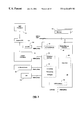
- FIG. 1 is system-level diagram of preferred embodiment.
- FIGS. 2A-B are block diagrams of first- and second-level switch respectively of present embodiment.
- FIG. 3 is general switch block diagram of present embodiment.
- FIG. 4 is general control-path diagram of present embodiment.
- FIG. 5 is general datapath diagram of present embodiment.
- FIGS. 6A-B are block diagrams of LAN interface and datapath interface respectively of present embodiment.
- FIGS. 7A-B are block diagrams of DMA transfer between local memory and packet memory, and processor access to packet memory respectively of present embodiment.
- FIGS. 8A-B are processor access to L 3 CAM memory and control memory respectively of present embodiment.
- FIGS. 9A-B are processor access to L 2 CAM memory, and LAN arbiter interaction with datapath respectively of present embodiment.
- FIGS. 10A-B are transmit queue management block (XQMB) interfaces and operation respectively of present embodiment.
- XQMB transmit queue management block
- FIG. 11 is DMA block diagram of present embodiment.
- FIG. 12 is flowchart of CPU-to-packet memory operation of present embodiment.
- FIG. 13 is flowchart of packet memory-to-CPU operation of present embodiment.
- FIG. 14 is block diagram of L 3 block interfaces of present embodiment.
- FIGS. 15A-B are flowcharts of age table maintenance of present embodiment.
- FIGS. 16A-B are flowcharts of search and lookup operations respectively of present embodiment.
- FIG. 17 is flowchart of packet reception of present embodiment.
- FIG. 1 is top-level overview diagram of system architecture for preferred embodiment.
- Multilayer switch device 6 couples local area network (LAN) workgroup hubs 2 through enterprise switching hub 4 to wide-area network (WAN) links through multiprotocol router 8 .
- Multilayer switch 6 and associated technique enables simultaneous wire-speed routing at Layer 3 (L 3 ), wire-speed switching at Layer 2 (L 2 ), and support multiple interfaces at Layer 1 (L 1 ), according to OSI reference model.
- System may be embodied using one or more integrated circuits (ASIC), RISC processor, and software, thereby providing wire-speed performance on various interfaces in various operational modes.
- ASIC integrated circuits
- RISC processor RISC processor
- System architecture comprises two-level distributed multilayer switch, preferably using 4-Gbps non-blocking switch fabric 6 .
- Multilayer (i.e., both L 2 and L 3 ) switch fabric is entirely contained within single ASIC capable of switching 3M pps or more.
- a 4 Gbps I/O bus connects one or more interface modules to the ASIC.
- the switch matrix is not necessarily integrated with the MAC layer, a wide range of interface types can be supported (i.e., both LAN and WAN).
- various combinations of layer 1 interfaces are supportable, and all interface modules are field-upgradable.
- Various interface modules may carry multiple physical interfaces.
- first-level switch 22 includes switch ASIC 20 , which couples RISC coprocessors (i.e., Network Management Processor (NWP) 10 and Route/Switch (RS) processor 12 ,) for supporting for higher-layer software functions and support features. Optional components may be added for redundancy of critical system components, such as power supplies. Memory 16 and input/output (I/O) modules 14 couple to switch circuit 20 .
- RISC coprocessors i.e., Network Management Processor (NWP) 10 and Route/Switch (RS) processor 12 ,
- NWP Network Management Processor
- RS Route/Switch
- Memory 16 and input/output (I/O) modules 14 couple to switch circuit 20 .
- second-level switch or cross-bar interconnection 18 couples multiple first-level switches 22 .
- aggregate performance of non-blocking switch fabric may exceed 24 Gbps.
- RISC processors 10 , 12 provided in each switch element 22 execute software to provide standards-based dynamic routing, and non-real time activities such as network management.
- Software is stored in flash memory, and is network-updatable via TFTP.
- Preferred software functions include: dynamic Internet Protocol (IP) routing (e.g., RIP, RIPv2, OSPF); layer 2 support (e.g., 802.1D STP); configuration support (e.g., enable/disable Layer 2 or Layer 3 support on per-port basis; ports can be grouped into broadcast domains, flexible subnet configuration); network management: (e.g., SNMP, HTML, Telnet, TFTP, DHCP support).
- IP Internet Protocol
- layer 2 support e.g. 802.1D STP
- configuration support e.g., enable/disable Layer 2 or Layer 3 support on per-port basis; ports can be grouped into broadcast domains, flexible subnet configuration
- network management e.g., SNMP, HTML, Telnet, TFTP
- QOS quality-of-service provisioning
- IP Multicast e.g., IGMP, DVMRP
- network traffic monitoring e.g., RMON
- hot standby support e.g., VRRP
- additional dynamic routing e.g., NHRP
- IEEE enhancements e.g., 802.1Q (i.e., VLAN), 802.3x (i.e., flow control), and 802.1p (i.e., priority)
- present multilayer switch system is suitable for applications at network aggregation points
- present system may also be used in high-performance workgroup and server applications.
- present system may interconnect between cluster of closely cooperating high performance computers, such as in video postproduction, where ability to transfer data rapidly between workstations is critical to production throughput.
- wire-speed performance is interesting, and flexible layer 3 -addressing support provides connections outside workgroup, without impacting switching speed.
- present multilayer switch system provides network attachment point for one or more servers. Wire-speed performance of present system allows network designer to use either layer 2 or layer 3 topologies, and removes potential network performance bottleneck.
- preferred implementation of innovative multilayer switch apparatus and methodology provides following functionality: support for 16 or more full-duplex 100BaseT ports or up to 28 ports of 10/100BaseT ports; direct interface to MIPS-type RISC processor for management and routing; integration of SDRAM controller for shared high-speed 6-channel packet memory; integrates of CAM access interface to system processor; integration of hardware CAM processor for L 2 learning, lookup and live interactive activities or transactions; integration of hardware hash-based IP header lookup and management; integration of hardware-based transmit and free queue management; integration of L 2 and L 3 forwarding of unicast, broadcast and multicast packets; broadcast traffic management; integration of QoS, with 4 priority queues per port; hardware-handled packet movement; integration of 768 bytes of dual-port memory for L 2 and L 3 header for 28 ports; support for 4 MB/16 MB of SDRAM packet memory; implementation of 256 bytes of data buffers for concurrent transfers to PM SDRAM and LAN bus; intelligent buffer scheduler & arbiter for efficient
- multilayer switch circuit 20 is implemented as single-chip integrated circuit (e.g., semicustom ASIC) for processing handles switching of any canonical packet, cell, frame, or other data communication element, with no or limited processing assistance from external processors.
- Switch circuit 20 operates in relatively low latency, and store-and-forward switching modes. Transactions between Ethernet ports may operate in low-latency cut-thru mode; other transactions may occur in store-and-forward mode.
- switch circuit 20 may contain substantially one or more of following functions: external bus interface, processor interface, CAM interface, LAN interface, packet memory (PM) SDRAM interface, route cache SDRAM interface, control memory (CM) SRAM interface, LAN block, LAN bus arbiter, LAN bus controller, LAN block interfaces, data path block, data path buffers, data path controller, buffer scheduler, packet memory, packet memory SDRAM arbiter and controller, DMA function-to-processor interface, packet engine (PE), port control function, port attribute memory, L 2 CAM engine, memory blocks for header and CAM analysis result, CAM structures, L 2 header analysis hardware engine, auto-forwarding block, forwarding block, L 3 header analysis result memory, free queue management block, block attributes management, transmit queue management block (XQMB), SRAM arbiter and controller, processor interface, L 3 block, L 3 header memory, hash function, L 3 lookup algorithm, L 3 management function, L 3 aging function, route cache (RC) SDRAM arbiter and controller, RISC processor interface, slave interface,
- switch system shows general logic block diagram for switch circuit 20 coupled to: 64-bit 66 Mhz LAN bus, external memory 16 through 32-bit 99-Mhz bus, L 2 CAM through 16-bit 66-Mhz bus, control memory 136 through 16-bit 66-Mhz bus, L 3 route cache through 16-bit 66-Mhz bus, and switch processor 12 through 16-bit 66-Mhz bus, which couples to network management processor (NMP) 10 through external interprocessor controller (IPC) 24 .
- NMP network management processor
- IPC interprocessor controller
- internal control path of switch circuit 20 is shown.
- External switch processor 12 couples to CAM interface 46 , free queue management 48 , L 3 lookup 50 , transmit queue management and scheduler 58 , SDRAM memory controller 62 , and SRAM memory controller 64 .
- internal control path includes forwarding engine 52 , which couples to CAM interface 46 , free queue management 48 , L 3 lookup 50 , block attributes 60 , transmit queue management and scheduler 58 , and receive block 54 .
- Transmit queue management and scheduler 58 couples to transmit block 56 , SRAM memory controller 64 , and block attributes 60 .
- Receive block 54 and transmit block 56 couple to LAN bus.
- CAM interface 46 couple to CAM bus and receive block 54 .
- SRAM memory controller 64 couples to free queue management 48 , block attributes 60 , L 3 lookup 50 , and SDRAM memory controller 62 .
- SDRAM memory controller 62 couples to RC memory bus and L 3 lookup 50 .
- Block attributes 60 couples to free queue management 48 .
- Forwarding engine 52 couples to receive block 54 .
- multi-channel packet memory arbiter and controller 66 couples to SDRAM packet memory bus, processor and DMA interface 68 , L 3 engine 70 , receiver buffers 72 , and transmit buffers 74 .
- Receive and transmit buffers 72 , 74 couple to media access controller (MAC) first-in first-out (FIFO) bus.
- MAC media access controller
- FIFO media access controller
- Switch circuit 20 includes processor interface 36 which couples to 32-bit MIPS RISC processor multiplexed bus (e.g., NEC R4300).
- processor bus a 32-bit address/data bus operable up to 66 Mhz, operates in master and slave modes.
- slave mode such processor bus responds to accesses to internal resources, such as registers, CAM 142 , Control Memory 136 , PM SDRAM and RC SDRAM.
- master mode such bus handles DMA operations to and from PM SDRAM.
- Such processor bus does not respond to accesses to external resources, but cooperates with external system controller circuit.
- master mode such processor bus may handle DMA to system memory.
- Switch circuit 20 includes CAM interface 46 , a dedicated 16-bit bus compliant with content-addressable memory (i.e., Music Semiconductor CAM 1480 compatible) operating at 66 Mhz. Such bus may be shared by external interface.
- CAM interface 46 a dedicated 16-bit bus compliant with content-addressable memory (i.e., Music Semiconductor CAM 1480 compatible) operating at 66 Mhz.
- Such bus may be shared by external interface.
- RS route/switch
- Switch circuit 20 For route/switch (RS) processor accesses to CAM memory, special data path is provided through switch circuit 20 .
- Switch circuit 20 generates CAM access timing control on behalf of RS processor 12 .
- Switch circuit 20 learns and looks-up MAC addresses and port numbers through such bus.
- Switch circuit 20 includes LAN interface 40 which couples LAN bus, a 64-bit access bus operating at 66 Mhz. Ethernet MAC devices connect to such LAN bus through receive and transmit MAC FIFO bus. Switch circuit 20 generates select signals and control signals for access to external MAC device FIFO bus. Switch circuit 20 reads/writes data in 64-bit single-cycle burst mode. Burst size is 64 bytes. Preferred bandwidth is 4 GB/s at 64-bit/66 Mhz-operation at 64-byte slice size. Ethernet frames are transferred across LAN bus. At end of receive frame, status bytes are read.
- Switch circuit 20 includes packet memory (PM) SDRAM interface 42 , which includes PM SDRAM bus which operates at 32-bit/99-Mhz standard. Packet memory 16 is directly connected to such bus through registered transceivers. Preferred bandwidth is 400 MB/s at 99-Mhz operation and 64-byte burst mode. Seven-channel arbiter inside switch circuit 20 allows up to 7 agents to access packet memory 16 . PM interface supports up to 8 MB of SDRAM in two banks.
- Switch circuit 20 includes interface to Route Cache (RC) SDRAM for coupling timing control signals and multiplexed 16-bit bus, which operates in 66-Mhz mode capable of streaming data at 132 MB/sec.
- RC Route Cache
- Switch circuit 20 includes interface to Control Memory (CM) SRAM for managing block free queue list, transmit queues, block parameters and L 3 CAM aging information.
- CM Control Memory
- Such interface is 16-bits wide and operates at 66-Mhz. Address and data buses are multiplexed and operate in flow-through and pipelined modes.
- FIG. 6A shows LAN block and interfaces 40 externally to Ethernet Media Access Controller (MAC) FIFO bus and internally to CAM interface block, datapath block 44 , and packet engine block 82 .
- LAN block interface functionality include bus arbitration for receive and transmit requests of FIFO bus, bus control and protocol handling, signaling internal datapath block to initiate data transfers and communicating with packet engine to signal begin and end of receive and transmit operations on FIFO bus.
- datapath block 44 couples to FIFO data bus, LAN bus controller 76 , buffer allocator 78 , and packet engine 82 .
- LAN bus controller (LBC) 76 couples to FIFO bus control, buffer allocator 78 , and receiver and transmit arbiters 80 , which couple to packet engine 82 and receive and transmit requests.
- LBC LAN bus controller
- LAN interface 40 When LAN interface 40 operates, receive requests and transmit requests are multiplexed and fed by external logic. Multiplexer uses 2-bit counter output. Front end demultiplexer reconstructs requests on 32-bit receive request register and 32-bit transmit request register. Few clocks latency for request may be sensed to be activated or deactivated, which may be handled by arbiter mechanism 80 .
- Receive arbiter 80 services receive port requests, preferably in round-robin scheme for equal distribution. Overlapped processing provides improved performance. Hence, if receive port is under service, next request prioritization occurs in parallel. During arbitration, arbiter 80 may receive port enabled, free block allocated signals from other modules. Upon certain channel winning arbitration, internal receive buffer is allocated 78 , and data staged from MAC FIFO bus for packet memory 16 . When buffer is granted, channel is presented to LAN Bus controller 76 for data transfer.
- transmit arbiter 80 services transmit port requests in round-robin scheme for equal distribution. Overlapped processing provides improved performance. Hence, when transmit port is under service, next request is prioritized in pipeline.
- arbiter 80 may receive port enabled, valid packet assigned, in link mode the transmitter has at least one slice signals from other modules. If channel has data slice in datapath 44 , channel is not allowed to join arbitration until data is put into packet memory 16 , thereby preventing out-of-sequence data transfer.
- Upon channel winning arbitration it is presented to buffer allocator block 78 to obtain internal transmit buffers for staging from packet memory 16 for MAC FIFO bus. Once transmit request wins arbitration, and transmit buffer is allocated, channel is presented to packet engine block 82 to obtain data from packet memory 16 . Once data is staged in transmit buffer, buffer requests to LAN Bus controller 76 to transfer data in transmit buffer to MAC FIFO bus.
- LAN bus controller 76 provides access to MAC FIFO bus targeted to port moving slice between MAC FIFO and internal data buffers. Receive request, which wins receive arbitration and secures one of receive buffers from buffer allocator 78 and transmit buffers having data for transfer to FIFO bus, competes for services of LAN bus controller 76 . Arbitration mechanism is configured to split bandwidth evenly between receive requests and transmit requests. LAN bus controller 76 generates end-of-packet status read cycles for receive request data transfer operations. Status information is used to determine if received packet is good or bad. If error is sensed, received packet may be rejected.
- Data bus width of LAN bus is 64 bits.
- LAN bus access is performed in burst mode (i.e., single-cycle burst mode) with maximum of 64-byte transfer, preferably executing at 8 data cycles in burst.
- LAN bus controller 76 is started by buffer scheduler when data buffer is allocated to receive or when data transfer from packet memory 16 to one of transmit buffers is complete.
- Receive and transmit data to LAN bus is staged through 64-byte deep receive and transmit data buffers in datapath block 44 .
- Receive and transmit requests arbitration and FIFO bus control are handled by LAN block.
- Buffer allocator 78 in datapath block 44 manages allocation of receive and transmit buffers, and packet engine block 82 handles movement of data between packet memory 16 and receive and transmit buffers.
- FIG. 6B shows datapath block 44 interface, including packet memory controller 82 coupled to data buffers 84 and packet memory engine (PME) 90 .
- Data buffers 84 couple to LAN block 86 , buffer scheduler 94 , slice counters 88 .
- Buffer attributes 92 couple to PME 90 and LAN block 86 , which couple to buffer scheduler 94 .
- Data transfers between packet memory bus and MAC FIFO bus are staged through receive and transmit buffers 84 in datapath block 44 .
- Block logic tracks state of buffers 84 .
- Datapath block 44 interacts with LAN Block 86 , packet engine block 82 and packet memory controller 82 .
- Buffers 84 match difference in bus access bandwidth for slice, and maintain concurrent transfers between FIFO bus and PM bus.
- Two buffers are provided for transmission, and two buffers are provided for reception. Such buffers are associated with respective buffer status. Transmit buffers hold data form PM 16 to MAC FIFO (LAN) bus. Receive buffers hold data from MAC FIFO bus to PM 16 . Each buffer has dedicated channel to PM SDRAM Controller. PM SDRAM Controller arbitrates each request to transfer on first-come/first-serve basis. On LAN side, appropriate buffer is selected for read or write.
- Frame transfer across LAN bus occurs on slice basis.
- Slice is 64bytes.
- burst data transfer size is slice size, except for last slice in frame.
- Last slice size is decided by frame size. Ports are serviced, in time-division multiplex mode.
- Receive slice buffer is used to capture LAN data from MAC FIFO.
- Slice is 64 bytes.
- Switch circuit 20 has two 64-byte buffers.
- incoming 64-bit data words are strobed on selected slice buffers, word-by-word, during clock edges. Write order is from top to down.
- Receive status is maintained for respective receive slice. For example, slice status provides:
- Receive slice size (represented by 6-bit number.) Maximum is 64 bytes.
- MAC provides in each data phase, valid bytes through bits (e.g., LBE# ⁇ 7 - 0 >).
- LBEI# ⁇ 7 - 0 > are registered and analyzed at end of data phase to provide cumulative slice size.
- MAC provides in each read data phase, if end-of-frame.
- EOFI# signal is registered and stored for EOF status. It is also used to close current transfer.
- SOF signaling The MAC provides on each read data phase, if Start-of-frame. SOFI# signal is registered and stored for SOF status.
- Transmit slice buffer is used to capture (e.g., PMDO) bus data and supply to LAN bus.
- Slice is 64-bytes.
- Switch circuit has two 64-byte slice buffers.
- 64-bit data words are read from selected slice buffer.
- One clock pre-read is implemented to provide minimum delay time on LAN data (LD) bus. Read order is from top to down.
- LD LAN data
- Status is maintained for respective transmit slice.
- Slice status is loaded by PM engine 90 when moving slice from PM.
- Status information includes:
- Slice size (represented by 6-bit number.) Maximum is 64 bytes.
- PM engine registers slice size.
- PM engine 90 registers signal while transferring slice from PM bus. If status is on, LAN FIFO controller asserts EOF# signal at appropriate data phase.
- PM engine registers signal while transferring first slice of packet from PM. If status is on, LAN FIFO controller asserts the SOF# signal at first data phase.
- Buffer scheduler 94 allocates transmit and receive data buffers to requesting agents, keeps track of busy/free status of each buffer, and allocates free buffer to requesting agent. Buffer scheduler 94 optimizes for (a) equal distribution of bandwidth between receivers and transmitters, (b) avoiding deadlock situation of transmit buffer, and (c) achieving highest concurrence of LAN bus and PM bus.
- Datapath controller includes buffer attributes 92 for receive and transmit buffers 84 , and track byte count per slice basis.
- Buffer attributes 92 such as End-of-Packet (EOF), start-of-packet (SOF), Byte Enables (BEB), and Slice Count are tracked from time data arrives into receive or transmit buffer until data leaves buffer.
- Buffer attribute 92 information is used by packet memory engine 90 to track progress of packet flowing through switch circuit 20 per slice basis.
- Datapath controller interacts with buffer scheduler 94 at end of slice transfer to release buffer. Synchronization between PM SDRAM controller and LAN bus interface 40 is thereby accomplished.
- Packet memory resides on dedicated SDRAM bus.
- Switch circuit 20 integrates SDRAM controller to access packet memory 16 .
- PM SDRAM controller functionality includes: 32-bit interface operating at 99-Mhz to 8 MB of external SDRAM; support for up to 7 internal requesting agents; arbitrates requests and generates request to SDRAM control block; pipelines requests for maximum efficiency and throughput; bursts of 4 (one bank), 8 or 16 (both banks) accesses on SDRAM; and maximum performance at 16 bursts and minimum performance at single read or write.
- Route processing is provided by MIPS R4000 family RISC processor 12 , which interfaces with switch circuit through address/data multiplexed bus.
- RISC processor interface may use external system controller, for example, for communicating with switch circuit 20 though processor slave port.
- RISC processor serves switch or route processor 12 .
- Several register resources in switch circuit 20 are used by RISC processor 12 to control configuration and operation of switch circuit 20 .
- RISC processor 20 may access resources outside of switch circuit 20 , such access being controlled by switch circuit 20 packet memory 16 , route cache memory, and CAM for L 2 forwarding.
- Switch circuit 20 communicates status of operation and draws attention of processor 12 through status and process attention registers. When configured, switch circuit 20 performs DMA of data from packet memory to processor local memory, and forwards packets to processor queue maintained by switch circuit 20 .
- route processor (RP) 12 is NEC Vr4300 RISC microprocessor from MIPS family with internal operating frequency of 133 Mhz and system bus frequency of 66 Mhz.
- Processor 12 has 32-bit address/data multiplexed bus, 5-bit command bus for processor requests and data identification, six handshake signals for communication with external agents, and five interrupts. Bus width can be selected as 32-bit operation.
- Processor 12 supports 1, 2, 3 and 4-byte single accesses and 2, 4 and 8 word burst accesses. Processor 12 uses little endian when accessing switch resources.
- RP 12 is interfaced to switch circuit 20 .
- RP 12 communicates with NMP 10 through interprocessor communication (IPC) bus 24 , and accesses switch local resources, such as packet memory 16 , L 3 CAM (Route Cache) 28 , control memory 136 and L 2 CAM 142 through switch circuit 20 and local resources, such as local memory, ROM etc., through system controller.
- IPC interprocessor communication
- switch local resources such as packet memory 16 , L 3 CAM (Route Cache) 28 , control memory 136 and L 2 CAM 142
- switch circuit 20 and local resources, such as local memory, ROM etc.
- Two interrupts are used by switch circuit 20 to issue interrupt requests to processor 12 .
- Two slaves on RP processor 12 system bus are switch and system controller.
- Switch is final agent to provide ready signal to processor requests that switch or system controller is ready to accept. During DMA transfer, switch acts as master.
- Write access is implemented as ‘dump and run’ with two pipelined buffers to improve system performance. This allows two back-to-back write cycles.
- One read request is processed at a time.
- Processor 12 accesses internal registers resources in 32-bit mode.
- Write buffer and read buffer are provided to packet memory 16 to match frequency difference of 99-Mhz and 66-Mhz.
- Memory interface to switch is 32-bit.
- Maximum burst size to packet memory 16 is four 32-bit words (i.e., 16 bytes).
- Read buffers are provided to L 3 CAM and control memory 136 because of 16-bit interface to switch. Little endian is used when data is packed and unpacked during write or read requests to 16-bit interfaced memories.
- Maximum burst size to L 3 CAM 28 is 16 bytes, and to CM is 8 bytes.
- Write or read request to memories is arbitrated through agents inside switch, such as forwarding engine, L 3 engine etc., so latency depends on various factors.
- processor 12 owns mastership or control of bus.
- processor 12 enters into uncompelled slave state after address phase, giving bus control to external agent to drive data.
- FIG. 7A illustrates DMA transfer between RP processor 12 local memory 100 and packet memory 16 .
- DMA transfer between packet memory 16 and NMP processor local memory is also provided in architecture.
- NMP processor system controller responds to DMA master requests between packet memory and NMP processor local memory.
- DMA is implemented using two design blocks called DMA engine 104 and DMA master 102 .
- DMA engine is interfaced to packet memory 16 and that of DMA Master to processor system bus.
- DMA is initiated by setting bits in DMA command register.
- DMA transfer between local memory 100 and packet memory 16 occurs substantially as follows:
- DMA engine 104 notifies DMA master 102 to initiate DMA transfer when packet is pending by giving request.
- DMA master 102 arbitrates for processor bus with RP processor 12 as another master by giving request (e.g., EREQ) to processor 12 .
- switch circuit 20 acts as master to system controller 98 .
- Processor gives bus control to RP processor when ready.
- bus is granted by processor, DMA transfer begins. Mastership of processor bus can be re-acquired by RP processor 12 between each slice transfer, which is maximum of eight 32-bit words (i.e., 32 bytes).
- DMA engine 104 reasserts request after each slice transfer, until block of packet data is transferred. At end of DMA, bus control is given to processor.
- DMA master 102 When bus is in uncompelled slave state, DMA master 102 does not access processor system bus to simplify design. While DMA transfer is taking place on bus, system controller 98 does not drive bus, assuming bus in slave state.
- FIG. 7B illustrates RP processor 12 access to packet memory (PM) 16 through L 2 /L 3 switch circuit 20 .
- Switch interface to packet memory 16 is 32-bit, and maximum burst size is 16 bytes.
- Synchronous DRAM is chosen for packet memory that can be operated at 66-Mhz, 99-Mhz and 125-Mhz frequencies.
- processor write request processor dumps write-data into front-end pipeline buffers 106 .
- Slave state machine 108 provides such data into packet memory write buffer 110 .
- Processor request is arbitrated with LAN requests and L 3 engine requests in PM SDRAM arbiter to access PM 16 .
- PM SDRAM controller 112 generates control signals for SDRAM.
- PM read buffer 114 During processor read request, read-data is provided in PM read buffer 114 from packet memory bus. Synchronizer 116 converts 99-Mhz signal into 66-Mhz pulse signal that initiates slave state machine to empty read buffer. Read data is muxed with data from other blocks and driven to processor system bus. Packet memory to local memory (PM-to-LM) DMA transfer data is not written into read buffer, but passed to processor system bus.
- PM-to-LM Packet memory to local memory
- FIG. 8A illustrates RP processor 12 access to L 3 CAM (route cache) memory 28 .
- RP processor 12 accesses L 3 CAM 28 through switch circuit 20 to initialize entries and maintain data structures.
- FIG. 8B shows control memory 136 access through switch circuit 20 .
- RP processor 12 couples to switch circuit 20 through 66-Mhz, 32-bit processor system bus, wherein pipeline buffers 106 receive processor write data and couple to slave state machine 108 .
- L 3 CAM write buffer couples to slave machine 108 and L 3 CAM SDRAM controller 120 , which receive requests from other agents and couples to L 3 CAM memory 28 through 66-Mhz, 16-bit bus.
- L 3 CAM read buffer 122 provides read data through 32-bit processor bus and couples to slave state machine 108 and register 134 over 16-bit bus.
- Register 134 receives 66-Mhz clock signal and couples to L 3 CAM memory 28 through 66-Mhz, 16-bit bus.
- CM write buffer 128 couples to slave machine 108 and CM SSRAM controller 130 , which receive requests from other agents and couples to control memory 136 through 66-Mhz, 16-bit bus.
- CM read buffer 132 provides read data through 32-bit processor bus and couples to slave state machine 108 and register 124 over 16-bit bus.
- Register 124 receives 66-Mhz clock signal and couples to control memory 136 through 66-Mhz, 16-bit bus.
- Synchronous SDRAM is chosen for L 3 CAM 28
- Synchronous SRAM is chosen for control memory 136
- Switch interface to both memories is 16-bit, and both memories operate at 66-Mhz.
- Processor 12 access to memories is similar in both cases, maximum burst size to L 3 CAM memory is 16 bytes, and maximum burst size for control memory 136 is 8 bytes. Data is packed and unpacked for each processor access.
- Each memory 28 , 136 has write buffer 118 into which processor write-data is provided from pipeline buffers 106 by slave state machine 108 . Since memory interface is 16-bit, processor write data is divided into two 16-bit half words.
- Processor 12 request to L 3 CAM memory 28 is arbitrated with L 3 engine requests.
- Processor 12 request to control memory is arbitrated with forwarding engine, FQMB, L 3 engine, XQMB, BAM and DMA.
- FQMB forwarding engine
- L 3 engine L 3 engine
- XQMB XQMB
- BAM DMA
- DMA forwarding engine
- L 3 CAM or CM read data from memory bus is provided in read buffer.
- slave state machine 108 starts emptying read buffer 122 appropriately and packs two half words into 32-bit word, and puts on processor system bus.
- RP processor 12 accesses L 2 CAM memory 142 through switch circuit 20 .
- Content Addressable Memory CAM
- Switch circuit 20 interface to L 2 CAM memory is 16-bit.
- Processor 12 executes commands write/read and data write/read to L 2 CAM 142 using CAM access registers provided inside switch circuit 20 .
- Processor 12 accesses L 2 CAM 142 through register-based request-grant handshake by loading L 2 CAM Access Control & Status Register to execute processing cycles.
- RP processor 12 arbitrates with CAM arbiter 138 in switch circuit 20 for CAM bus.
- slave state machine 108 For processor requests, slave state machine 108 generates control signals for CAM 142 , and CAM arbiter engine 138 processes switch requests.
- processor 12 provides write-data in pipeline buffers 106 .
- slave state machine 108 puts data from pipeline buffer 106 on CAM bus.
- read-data from CAM bus is muxed 140 with data from other blocks and passed to processor system bus. Write/read buffers need not be provided in present case.
- FIG. 9B shows LAN arbiters interaction with datapath.
- Register files 144 for receivers and transmitters including corresponding block address registers and byte count registers, couple to block address register and byte count register coupled to state machines 148 , which couple to switch data path 44 and receive and transmit arbiter 150 .
- Packet switch engine 82 performs control functions for transfer request in and out of receive and transmit buffer to packet memory 16 .
- Packet engine 82 handles LAN data movement, command process, and PM address calculation.
- packet memory engine 82 sets up for moving slice between packet memory 16 and allocated data buffer. This is triggered by scheduler while slice is scheduled to move in/out of data buffer. PM engine has access right to block address registers and registers to understand actual address on PM 16 and update packet size.
- packet memory engine 82 executes systematic hardware processes when Forwarding Block and Transmit Queue Management Block (FB/TQMB) generates instructions such as: link, receive enable, transmit enable, receive reject, etc. Hence, end of packet reception/transmission is noticed for next packet initialization. In notifying such events, priority encoding is provided for first-in/first-service integrity.
- FB/TQMB Forwarding Block and Transmit Queue Management Block
- packet memory engine 82 regards Ethernet ports as 32 concurrent full-duplex DMA channels. Relevant PM pointers for each channel are maintained. For every slice transfer, PM bus address is calculated.
- buffer attributes 92 are provided in attribute block address array, which is 3-port architecture having 64 ⁇ 12-bit 3-port memory array.
- Port- 1 is write port; port- 2 is read port; and port- 3 is read port.
- Packet memory engine 82 can write/read memory locations using various ports.
- Forwarding engine (FE) can read locations asynchronously.
- Port- 3 is assigned for FE.
- PM Engine 82 initializes block address for receive/transmit ports on command of Auto Forwarding Block. PM engine 82 reads block address relevant to receive/transmit port under service. PM engine 82 uses block address to identify packet in PM 16 .
- CAM interface block analyzes incoming packet at layer 2 , i.e., at MAC layer. Analysis result is forwarded to Auto Forwarding Block state machine. CAM processor is called for attention when ether header block is loaded in ether header memory. On such trigger condition, after acquiring CAM bus interface, CAM Processor starts defined fast processing action. Block contains layer 2 header memory, analyzed and to be analyzed port FiFOs, and result memory. CAM block interfaces to internal memories organized as memories and FIFOs as well as external CAM to accomplish L 2 lookup.
- begin of header When begin transfer of receive data, begin of header is identified and required header information is loaded into ether header memory. Sixteen-byte header blocks are reserved for each port in header memory. Loaded indication is updated on 5-bit entry in 32-deep ether header to-be-analyzed FIFO. Such FIFO provides first-in/first-service feature.
- Ether header memory is 2-port memory has 64 ⁇ 64 bit architecture. Port- 1 is write port, and port- 2 is read port. Such memory is located on LAN side of receive buffer. As first slice of new receive packet is loaded into receive buffer, header slice (i.e., 16 bytes) is written to ether header memory in 64-bit words. Ether port number is used as reference address to select header block number. Maximum of 32 header blocks can be stored in such memory. Port- 2 is used by CAM processing engine. CAM engine reads 16-bit quantity at a time through front-end 64:16 multiplexer. L 3 header information, up to 8 bytes per port is stored in different memory. Such information is used by L 3 lookup engine during routing operation.
- Ether-to-be-analyzed FIFO memory is 32 ⁇ 5-bit two-port memory, holding maximum of 32 port numbers to be analyzed.
- Port- 1 is write port
- port- 2 is read port.
- FIFO is written with port number when first slice of data is received on LAN bus and header loaded in ether header memory.
- CAM Processor reads port number through port 2 for indexing header memory.
- FIFO structure ensures that ports to be analyzed are presented to CAM engine in arrived order.
- Ether analyzed FIFO memory is 32 ⁇ 6-bit two-port memory, holding maximum 32 analyzed port numbers. Port- 1 is write port, and port- 2 is read port. CAM Processor writes analyzed port number through port- 1 and Forwarding Engine (FE) reads through port- 2 . FIFO structure ensures that analyzed ports are presented to forwarding engine in arrived order.
- FE Forwarding Engine
- Ether result memory is 32 ⁇ 16-bit two-port memory, holding results for 32 ether ports.
- Port- 1 is write port
- port- 2 is read port.
- CAM Processor writes L 2 forwarding result through port- 1
- FB Forwarding Block
- FB reads port number from Analyzed FIFO to make forwarding decision.
- FB uses port number as reference address to read CAM analysis result.
- External CAM memory is 1024 ⁇ 64-bit capacity on standard configuration. Size can be expanded to 2048 ⁇ 64-bit by adding CAM device in vertical expansion.
- CAM memory is connected on dedicated CAM bus. Such bus is shared between CPU and switch circuit. Normally such bus is default-owned by switch circuit. CPU can use bus by register mode bus handshake.
- CAM memory contains 1024 locations of 64 bits wide. Locations can be assigned as RAM property or CAM property. Location assigned as RAM will not be accounted in lookup process; CAM locations participate in lookup process. Repeatedly used parameters are stored in RAM so that real-time data movement between RAM location and Comparand/mask registers/etc. can happen with minimum overhead. Every location has associated status filed which describes entry, such as: empty entry, valid entry, skip entry on lookup, and RAM entry.
- Layer 2 header analysis is performed by CAM processor. Ethernet headers are loaded and processed on dedicated Ethernet header memory having 128 ⁇ 32 bit dual port memory. Assuming case where packet received on port(x), switch circuit 20 is triggered on such packet by request from MAC port number(x), which is effectively hardware packet arrival notification.
- Header is extracted from MAC received data stream. New receive packet data is identified with arrival of SOF, and first 16 bytes are treated as layer- 2 header. If header is concurrent to store access to receive buffer, then header is stored in port-specific block number(x) in header memory. Writing process may not account for port contention. Block written on port- 1 may not be accessed on port- 2 . Header is stored as header block(x). At end of storage, port number is written in ether-to-be-analyzed FIFO, which is 32 ⁇ 5-bit register. FIFO write pointer is incremented after each status write
- CAM processor starts when valid entry is loaded in Ether-to-be-analyzed FIFO. CAM Processor maintains read pointer to read valid entry. Valid entry is notified if there is difference between write pointer and read pointer. Entry read provides port number of header. CAM Processor uses port number to reach header block(x).
- switch system has 32 ports and 32 entries. New packet on port can not be received unless old packet is processed, according to system-level handshake. Hence, at any time, no more than 32 headers/header status may be stored, effectively reducing complexity of FIFO design. PM engine can blindly write header/status without looking for FIFO-full condition. CAM Processor can start as long as pointers are not equal.
- CAM processor handles header processing. CAM processor is notified of Ethernet header valid when write pointer and read pointer differ. When entry is valid on Ethernet-to-be-analyzed FIFO, CAM processor reads entry and increments read pointer. Using such value, CAM processor can reach specified header block. Ether header memory is divided into 32 blocks. Port number directly provides starting address of header block. Entries in block are consecutive 16 bytes.
- CAM processor processes header block, and writes result on port specific location on Ether result memory. CAM process completion is notified to Auto Forwarding Block through Ethernet result FIFO, which is 32 deep register construction. Each entry is 6-bit wide. Entry is result of CAM memory lookup. If set, destination MAC address indicates CAM hit. Routing tag in header block is valid. If clear, CAM lookup fails; routing tag does not contain valid information.
- CAM processor To write on result FIFO, CAM processor has write pointer, which is 5-bit counter. CAM processor write entry, whereas AFB read entry. When CAM completes process, it writes result entry, and increments write pointer. At last, CAM processor increments Ether header status FIFO read pointer to point to next entry.
- CAM processor header processing includes learning process of: source lookup, source port read, and source learning.
- CAM processor learns MAC addresses arriving from Ethernet ports. As associated process of CAM lookup, CAM processor determines whether source address was learned previously, i.e., by reading source address from Ether header memory, and writes CAM for lookup. If match occurs, processor presumes source port was learned; it reads existing port information from associated data to compare whether port is same as receiving port. If MAC header matches, whether or not ports match, processor makes entry live and at same time re-learns receiving port. If receiving port number does not match learned port, Source Address (SA) Learned flag is set. If miss, processor learns entry into next free address if CAM is not full, and if learned SA Learned flag is set. While updating such new entry, processor follows correct data structure for RAM associated information.
- SA Source Address
- attribute is set with (e.g., ETHR_LRN_INHIBIT) register for each port to inhibit learning on specified ports. If set, during source lookup process, after source port read, entry is made live if hit and if miss, MAC address is not learned. Source port read phase can be skipped if source port filtering is not required.
- ETHR_LRN_INHIBIT e.g., ETHR_LRN_INHIBIT
- Destination lookup process includes steps: destination lookup and destination port read.
- CAM processor reads 6-bytes destination MAC address from header memory and writes on CAM for comparison lookup. If miss, destination is assumed unknown; if hit, destination is available through memory (e.g., ARAM) field, which provides destination port number and port/MAC address specific status and control flags. If hit, CAM processor reads ARAM field and writes in result memory, setting hit flag. If miss, CAM processor has nothing to read and write miss flag to result memory. Rest of result data is not valid in miss case. Forwarding blocks read this field for analysis and forwarding decision. At end of process, CAM analysis done flag is set for packet on receiving port.
- CAM processor analyzes results of source lookup and destination lookup processes to determine how to process incoming packet.
- Each port has two bits allocated to handle spanning-tree protocol requirements. One bit is allocated for ‘Port Blocked State’ flag and other for ‘Learn Inhibit’ flag, which is used for learning of MAC addresses on receiving port.
- Port Blocked State’ flag is used for forwarding decision. Filtering bits in result from both source lookup and destination lookup along with port specific STP control bits relating to forwarding, source port and destination port read as result of destination lookup and read are considered.
- CAM processor sets CAM analysis completion status for receiving port. If destination lookup resulted in hit and destination port is one of physical LAN ports and cut-thru switching on port is enabled or CPU port, port number is written to Ether analyzed FIFO. CPU port is allowed to enable Layer 3 analysis parallel to packet reception. Result processing is done by Auto Forwarding Block (AFB). AFB is notified of CAM process completion through Ethernet Analyzed FIFO. AFB can read highest priority FIFO entry using hardware hidden read pointer. If read pointer and write pointer are different, one or more valid entries are available in Ethernet analyzed FIFO. AFB reads valid entry and gets port number. Reading entry increments read pointer, if present entry is valid.
- AFB Auto Forwarding Block
- AFB can access Ether result memory. Refer to Auto Forwarding Block section for details on AFB functionality. If CAM analysis resulted in miss or hit but packet can not be switched, AFB does not need to be notified until packet reception is complete. Hence, CAM processor merely sets CAM analysis completion flag for receiving port. AFB processes packet when both receive completion and CAM analysis completion set for receiving packet.
- Time stamp register provides variable granularity for aging.
- Processor uses instruction set provided by CAM device. Entries to be aged are processed in one instruction, though setup is required before executing instruction. In addition to status bits provided by CAM for every entry, 3 bits in RAM field are dedicated for aging information. Status provide by CAM are used to identify if entry is ‘Valid’, ‘Empty’, ‘Skip’ or ‘RAM only’. One of bits allocated in ARAM field is used to mark entry ‘Permanent’. Entries marked ‘Valid’ and not ‘Permanent’ are considered for aging. Additional two bits in ARAM filed provide flexibility to CPU to implement aging process.
- processor visits CAM to ageout entries, it searches CAM for entries with oldest time stamp. In search process, processor configures mask registers in CAM in such way that age bits enter comparison, and entries that are not ‘Valid’ and marked ‘Permanent’ do not enter comparison. In next instruction, processor can clear ‘Valid’ bits on matching locations to ‘Empty’ state. By doing so, oldest entries are marked empty. From that point, aged entries do not enter compare operation until made ‘Valid’ aging during normal learning process.
- latest time stamp e.g., ETHER CAM CONTROL
- Auto forwarding block is hardware Ethernet packet forwarding engine and queue processor.
- AFB analyzes incoming packet and may forward packet both at layer 2 and layer 3 . After forwarding analysis is done, AFB posts and maintains port queues.
- AFB may accept packets from processor interface and post packet in requested queues.
- AFB provides processing power on packet-by-packet and manages required information for integrity of packet routing strategy.
- AFB feeds initial setup information for each ether packet for each port to run data transaction.
- AFB functionality enables switch circuit 20 to perform forwarding and filtering without real-time assistance from processor 12 .
- Processing element is out of the datapath, and forwarding and filtering is done at line rate for supported ports.
- AFB functionality includes: free queue management, block attributes management, receive port management, forwarding and filtering, transmit queue management, quality-of-service (QoS) support, and control memory interface.
- QoS quality-of-service
- Forwarding function features port linking, wherein receive port is linked to transmit port before packet is fully received, thereby improving latency between received and transmitted packets.
- Port linking is accomplished in forwarding stage if conditions are suitable. For example, packet can cut-thru with unique destination, i.e. no more than one port is target destination for packet. Cut-thru enable bit are satisfied for certain values, such as: destination port, speed-matching logic, xmtPortEn, xmtPortNotBsy, xmtQNotVld and mirrNotVld. Data arrive speed should not exceed transmitting port speed. Transmitter should be ready to accept command. Transmitter may be busy transmitting data, or there may be packets waiting for queue transmit. Also, there should be minimum of data present in buffer before process can start or arbitration latency may result in transmit FIFO under-run condition. In such case, transmitter is linked but does not start transmitting data until required minimum data is received in packet memory.
- FIG. 10A shows Transmit Queue Management Block (XQMB) 154 , which is hardware block for managing transmit queue functions for switch circuit 20 .
- XQMB 154 couples to forwarding engine (FE) 52 , DMA Engine 104 , block attribute memory (BAM) 152 , PME 90 , queue attribute memory (e.g., AttrRAM) 156 , port AttrRAM 158 , and control memory 136 through interface 160 .
- FE forwarding engine
- BAM block attribute memory
- PME 90 queue attribute memory
- AttrRAM AttrRAM
- port AttrRAM 158 port AttrRAM 158
- control memory 136 control memory
- XQMB 154 functionality includes: initializing and managing transmit queues for each port; maintaining QOS parameters (i.e., tokens) for each port; queues (e.g., nQueues and dQueues) blocks to/from control memory transmitter queues; forwarding blocks to requesting transmitter; returning block numbers to BAM controller 152 ; forwarding multi/broadcast block in ‘background’; supporting 28 physical ports, 3 logical ports and multi/broadcast port; and using round-robin priority scheme to service requests.
- FIG. 10B shows queue processor state machine 162 , which couples to transmit arbiter 80 , block address and byte count registers 164 in control memory, and transmit queue 136 .
- FIG. 11 shows DMA engine 104 , which couples to CPU register 166 , CPU master interface 36 , XQMB 154 , packet memory interface 42 , and control memory interface 160 .
- DMA engine handles data transfer between packet memory 16 and CPU local memory 100 so that CPU 12 may perform other tasks.
- CPU 12 packet send is enabled by creating packet in local memory 100 , register set-up, and initiating packet transfer.
- packet receive is enabled by notifying CPU 12 .
- CPU 12 checks block attribute to determine whether to process packet. If CPU 12 transfers packet to local memory 100 , it DMA engine 104 is notified to proceed. Otherwise, register is written to de-queue packet.
- FIG. 12 flow chart shows CPU 12 to packet memory 16 operation. Initially, in software, CPU sets-up register and initiate packet transfer 168 . Then, in hardware, processor determines 170 whether to initialize block attribute 176 , whether 172 to initialize DMA transfer 178 , and whether 174 to write command to XQMB 180 .
- FIG. 13 flow chart shows packet memory 16 to CPU 12 operation. Initially, in hardware, block attribute is read 182 , and CPU 12 is notified 184 . Then, in software, run CPU check whether DMA needed 186 ; if not, then set register to de-queue 188 . Then, in hardware, DMA transfer 190 , and notify CPU 12 .
- FIG. 14 shows switch circuit 20 with L 3 engine 70 coupled to FE 52 , interface 36 to CPU 12 , interface 42 to packet memory 16 , IP header RAM 198 , MAC address RAM 196 , interface 194 to L 3 CAM 126 , and interface 160 to control memory 136 .
- L 3 check block captures destination IP address, Time To Live Field and Checksum field in L 3 Header Memory, for use by L 3 block 70 for L 3 lookup and processing.
- L 3 check block processes rest of packet header. Receive packet is checked for IP protocol filed, and to detect packets for specialized handling.
- IP header length is checked to determine whether packet needs specialized option processing. If header length is not equal to 5 32-bit words, option processing is applied to packet. Time To Live filed is checked to see if TTL field is more than 1; if less than 1, packet is marked with TTL error flag. IP packet length is checked for minimum length to contain full IP header. Checksum of header is performed.
- L 3 INFO Memory is 32-byte wide. Each location is dedicated for corresponding numbered port. Result of L 3 header checks for receiving port is stored in corresponding location and used by Forwarding Block to decide whether packet is sent to L 3 Block for processing.
- L 3 check (e.g., CHK) block takes into consideration if arriving packet contains VLAN tag, if VLAN tag option is enabled. If so, hardware accounts for shift in appropriate fields for L 3 header checking process. This amounts to 4-byte shift of L 3 header following MAC header.
- VLAN priority bits are extracted and passed along with L 3 INFO. VLAN priority bits may be enabled to override QoS information set in L 2 CAM result and L 3 Header Lookup result. Programmable register is provided to load pattern to identify if incoming packet is VLAN tagged packet.
- L 3 Engine (L 3 E) 73 is hardware block for implementing the Layer 3 CAM lookup and age table functions for switch circuit 20 .
- L 3 E 72 receives requests from forwarding engine (FE) 52 and CPU 12 , processes requests and returns results to requester.
- L 3 E 72 lookup functions includes: receiving, buffering and processing lookup requests from FE 52 ; providing hardware to calculate hash index from destination IP (DstIP) address provided by FE 52 ; reading CAM entry at address and checking for IP address match; following linked list entries until match is found or end of list is reached; and returns lookup result to FE 52 .
- DstIP destination IP
- L 3 E 72 age table maintenance function includes: maintaining age table in control memory 136 ; adding and deleting entries in table by CPU 12 request; aging table at CPU-controlled intervals; reporting aged entries to CPU; maintaining aging time stamp; and making entries live.
- L 3 E 72 CAM management assistance function includes: providing hardware hash calculation function for CPU 12 ; implementing search function which scans L 3 CAM and reports matching entries; and providing change option to search function which writes new data into matching entries.
- CPU 12 interface to L 3 Engine 70 is for age table and L 3 CAM maintenance.
- Initial CAM entries are written to L 3 CAM 126 by CPU 12 through dedicated control memory interface port. Managing linked entries and free buffers is done by CPU 12 . Searching for entries and reporting or changing them is accomplished by appropriate command registers.
- Age table entries are created and deleted by CPU 12 using add and delete commands. Aged entries are reported to CPU 12 and deleted by CPU 12 using delete command. Time hardware modifies age table entry when entry is made.
- Packet memory 16 includes 8-MB SDRAM with 4 1M ⁇ 16 devices providing 32-bit data path to 4096 2KB blocks for packet storage.
- L 3 Engine 70 writes to packet memory 16 to modify fields (e.g., destination address (DA), source address (SA), TTL and checksum) in packet following L 3 lookup.
- DA and SA fields are written in 32-byte burst with byte enables set appropriately.
- MAC address RAM 196 is 32-entry RAM, indexed by port number, which contains lower byte of MAC address for each physical port.
- IP HDR RAM 198 is 2-port Internet Protocol header memory RAM located on switch circuit 20 . Each entry contains IP values (e.g., TTL, checksum and DST IP) for packet. Write port of RAM 198 is used by packet memory engine 90 to store data from packet IP header. As data streams to packet memory 16 , appropriate bytes are pulled and written to RAM 198 . L 3 Engine 70 uses read port of RAM 198 to access data required to process lookup request from FE 52 . Entries are indexed by port number, so receive (RCV) port number is used to lookup entry.
- IP values e.g., TTL, checksum and DST IP
- Write port of RAM 198 is used by packet memory engine 90 to store data from packet IP header. As data streams to packet memory 16 , appropriate bytes are pulled and written to RAM 198 .
- L 3 Engine 70 uses read port of RAM 198 to access data required to process lookup request from FE 52 . Entries are indexed by port number, so receive (RCV) port number is used to lookup entry.
- L 3 CAM 126 is contained in 2-MBytes synchronous DRAM (SDRAM) located in single 1M ⁇ 16 part. Since SDRAM is optimized for burst transfer, L 3 Engine 70 accesses occur in bursts of eight 16-bit words. On-chip arbiter/controller logic for L 3 CAM 126 memory has multiple ports to allow better pipelining of accesses and L 3 engine 70 uses two of these ports.
- SDRAM 2-MBytes synchronous DRAM
- L 3 CAM 126 data structure is implemented as hash table combined with pool of free buffers which can be linked to entry in hash table. Entry, whether in hash table or free buffer pool, is 8 words (16 bytes). Entry is referred to by entry number, 17-bit number used when indexing CAM, when indexing into age table or when reporting results of search or aging operation.
- Base hash table contains 64K entries and resides in lower 1-MByte SDRAM. Entries in table have entry numbers in 0 to 64K range, i.e. bit 16 of entry number is set to ‘0’. Entries located in free buffer pool are in upper 1-Mbyte of SDRAM, and entry numbers have bit 16 set to ‘1’. Address of first word of entry in CAM is determined by concatenating entry number with 3 bits of ‘0’.
- CPU 12 creates entries in hash table for DstIP addresses by hashing address and using resulting 16-bit hash index as offset to entry in table. When multiple address' hash to same entry in base table, link is created to free buffer pool entry. If additional addresses hash to same location, they can be added to end of linked list. CPU 12 creates and maintains entries and manages linked list structures.
- Control memory block (CTL MEM) 136 uses 128K ⁇ 16 synchronous SRAM (SSRAM), instead of SDRAM devices because most data structures stored require single read and write accesses.
- L 3 Engine 70 uses 32-KB portion of control memory to store age table. It does single read followed by single write of word in age table. Each 16-bit word contains age table information for 4 CAM entries. Aging information for particular L 3 CAM 126 entry is accessed by using CAM entry number divided by 4 as address into age table.
- FE 52 performs lookup requests to L 3 Engine 70 for each IP packet to be processed. Four-deep FIFO buffer is provided to buffer these requests. FE 52 provides RCV Port Number and Block Number for each packet. After lookup is complete, L 3 Engine 70 returns RCV Port Number as well as L 3 Result and L 3 Status word containing various flags and information from matching CAM entry.
- age table support since control memory 136 containing age table does not support locked operations, table modifications are done by hardware. Such table modifications address condition of two agents trying to modify same table entry.
- CPU 12 can initialize entries to invalid state at startup by writing to control memory; but during operation, hardware performs table modifications.
- Age table operations are done by CPU 12 write to age command register.
- Write to age command register causes Age Table Busy flag in L 3 Status register to be set until operation is complete.
- Aged entries are reported in registers (e.g., AgeResult 1 & 2 ).
- age table maintenance is illustrated, starting with CPU or live command processing 200 , then determine if age command 202 applies. If so, increment time stamp 210 and set age flag; otherwise, read table entry 204 , mask and modify table entry 206 , and write table entry 208 . Further, in FIG. 15B, after age flag set 212 , age table is read 216 , then determine age out 218 . If so, then write result registers 220 , set result valid 222 , wait for CPU 224 , and clear result valid 226 ; otherwise determine 228 if last entry. Next, clear age flag 232 , 230 and read hash table 240 .
- Time stamp is 2-bit value providing four age time intervals. There are two age time counters, currTime and ageTime. CurrTime is reset to zero and increments when CPU 12 issues age command. Entries with time stamps equal to this value are newest entries. AgeTime value is always equal to currTime+1 (i.e., currTime ⁇ 3, modulo 4 ). Entries with time stamps equal to ageTime are aged next time CPU 12 issues age command.
- CPU 12 adds entry to age table when creating new entry in L 3 CAM 126 . Until entry is added to age table, entry does not participate in aging process.
- CPU 12 writes (e.g., AgeCmd) register with entry number and add or add permanent command, and hardware reads appropriate entry, modifies valid and permanent bits appropriately and writes currTime into time stamp field.
- Hardware makes entry live (i.e., accessed) when L 3 CAM lookup results in IP hit. Entry number of matching entry is used to access age table, and time stamp field is updated with currTime. Entries which are accessed frequently have more recent time stamp than infrequently used entries, and are not aged out.
- CPU 12 deletes entry in age table when removing entry from L 3 CAM 126 .
- CPU 12 writes AgeCmd register with entry number and delete command, and hardware reads appropriate entry, clears valid bit, and writes modified entry back to table.
- AgeCmd register When CPU 12 age timer expires, CPU writes AgeCmd register to initiate aging process. This sets AgeCmd Busy bit in L 3 Status register until entire table is aged. Add and delete commands can be issued, but new age commands have no affect.
- ageCmd register When CPU writes ageCmd register, hardware increments ageTime and currTime counters and resets aging address counter to zero. Hardware reads 32K words of age table and checks if any time stamp fields are equal to ageTime. Entries with time stamps equal to ageTime are reported to CPU 12 as aged out. CPU 12 deletes aged entry from CAM and age table.
- Age Result Valid bit is set in L 3 Status register, and aging process is halted until result is read by CPU 12 . Reading AgeResult register restarts aging process and clears status register bit.
- First aged entry number used to access L 3 CAM 126 to retrieve DstIP for entry.
- DstIP is hashed to locate base hash table entry and CAM entry at address is read.
- Hardware follows linked list, reading CAM entries until retrieving entry with Link Address equal to original aged entry number. Entry number is reported along with aged entry number in AgeResult registers.
- CPU 12 provides L 3 CAM management functions, including initial setup, adding entries, deleting entries and managing linked lists and free buffer pool.
- Hardware provides automatic search/change capability to assist CPU 12 in locating entries with certain characteristics and optionally changing such entries.
- Search operations are initiated by CPU 12 write to SearchCmd register.
- Write to SearchCmd register causes Search Busy flag in L 3 Status register to set until operation is complete.
- Matching entries are reported in (e.g., SearchResult) registers.
- FIG. 16A shows search operation steps.
- CPU initiates search 234 , writes commands 236 , initialize entry to zero 238 , read hash table 240 , then determine match 242 . If so, write result to registers 244 , and wait for CPU 246 ; otherwise, determine if linked 248 . If so, clear age flag 250 , else, determine if last entry 254 . If so, clear age flag 252 ; otherwise, clear age flag 256 .
- Hardware performs automatic and exhaustive search of L 3 CAM 126 when SearchCmd register is written. Starting with entry 0 , each entry in base hash table is read and checked against search criteria. If entries have valid link address, then linked entries are read and checked. Minimum 64K CAM entries are read.
- SearchCmd can be written with Abort Flag set, and hardware exits search process. Pending SearchResults are read by CPU 12 before hardware exists and clears Search Busy flag.
- SearchMask and SearchData registers (16 registers total). Before search command is issued, SearchMask registers are written. ‘0’ in bit position masks bit from consideration in comparison. SearchData registers are written with data values to be matched. Registers containing data to be matched are written.
- ChangeMask and ChangeData registers (16 registers total).
- ChangeMask registers are written. ‘1’ in bit position marks bits to be changed.
- ChangeData registers are written with desired new data values. Registers containing data to be changed are written.
- NewCamDataX ChangeMaskX & ChangeDataX
- L 3 Engine receives CAM lookup requests from forwarding engine and searches matching entry in L 3 CAM 126 . Results of search are returned to FE 52 , and additional requests are serviced.
- flow chart shows CAM lookup steps. Initially, valid buffer is set 258 , read IP header RAM 260 , hash destination IP (DstIP) address 262 , and read hash table 264 , then determine if valid and hit 266 . If so, read port MAC RAM 268 , update packet data 270 , modify packet 272 , and write result 274 . If not, determine valid link 276 . If so, follow link 278 and read hash table 264 , else write result 274 .
- DstIP hash destination IP
- L 3 Engine 70 buffers up to 4 lookup requests from forwarding engine (FE) 52 . When buffer is full, busy signal is sent to FE 52 . Buffer is organized as FIFO and contains receiving port number and block number for lookup request.
- DstIP address is hashed to 16-bit value which is used as entry number for base hash table. That entry is read, and words containing DstIP address are compared to packets DstIP address. If these two addresses match, then IP hit bit is set, and results of successful lookup are returned to FE 52 .
- packet Before result is posted to FE 52 , packet may be modified, depending on bit in L 3 Flags field of CAM entry. If Don't modify bit of CAM entry is set, nothing is changed in packet. Otherwise, when lookup is successful, TTL field of IP header is decremented and modified in packet memory, and (e.g., CheckSum) field is recalculated and changed. Packets DA is overwritten with value contained in matching CAM entry, and SA is replaced with value from MAC Address Registers and MAC Address RAM.
- L 3 Flags field of CAM entry If Don't modify bit of CAM entry is set, nothing is changed in packet. Otherwise, when lookup is successful, TTL field of IP header is decremented and modified in packet memory, and (e.g., CheckSum) field is recalculated and changed. Packets DA is overwritten with value contained in matching CAM entry, and SA is replaced with value from MAC Address Registers and MAC Address RAM.
- L 3 CAM 126 hardware checks to see if default route registers are written by CPU. These registers provide ‘default route’ CAM entry and are programmed with same information as CAM entries in control memory 136 . If default route exists, then packet is modified using default information, and (e.g., IPHit and DefaultRouteUsed) bits of L 3 Result are set.
- default route registers are written by CPU. These registers provide ‘default route’ CAM entry and are programmed with same information as CAM entries in control memory 136 . If default route exists, then packet is modified using default information, and (e.g., IPHit and DefaultRouteUsed) bits of L 3 Result are set.
- Upper bits of MAC address for ports are provided in three registers. Three 16-bit registers provide full 48-bits address, but lower byte of address for each port is provided by MAC Address RAM 196 .
- MAC Address RAM 196 contains lower byte of MAC address for each port. It is 32 ⁇ 8 dual port ram which is written by CPU 12 and read by hardware during packet modification. This value replaces lower byte from MAC Address Registers when writing new SA for packet.
- L 3 results of CAM lookup returned to FE include receive port number and block number originally provided by FE 52 and two 16-bit values, L 3 Result and L 3 Status. A detailed bit definition for these last two values was provided earlier in this document.
- Switch circuit 20 operates on various performance and integrity levels. In cut-thru switching mode, relatively fast ether switching mode and high performance level are achieved; however, there is possibility of transmitting packet with error during receive process. In this mode, CPU programs MACs to raise receive request when collecting 64 bytes. Also it programs MAC to raise subsequent receive request after every 64 bytes collection. First request provides fast header analysis and switching.
- SF store forward
- Switch circuit 20 waits until packet completion and updates transmit queues of relevant destination. MAC programming remains same.
- Forwarding Block acts on ‘store forward mode’ mode on port by port basis. SF mode is selectable as per port basis. In this mode port linking is disabled.
- packet moves in following directions: received on LAN port(x) and transmitted to any/all other LAN ports; received on LAN port(x) and posted to UL queue; received on LAN port(x) and posted to CPU queue; received on LAN port(x) and packet dropped; and forwarded from CPU to any/all LAN ports.
- packet flows through packet memory 16 and switch circuit 20 .
- switch circuit 20 participates in forwarding, filtering and queue management.
- switch circuit 20 In case of Ethernet port originated packet flow, packet is received on Ethernet ports, and switch circuit 20 is triggered on such packet from request from one of MACs. This is hardware trigger mode. Switch circuit 20 , in coordination with RISC processor 12 , allocates free block pulled from receive free list. Once block is assigned, block is busy until destination agent(s) complete transmission. Transmission completion has mechanism to release block and insert in receive free list.
- switch circuit 20 needs to obtain packet header information. Header is extracted from MAC received data stream.
- PM engine 90 identifies header from data stream and loads on port-specific segment of Ether header memory.
- CAM Processor makes lookup on CAM and delivers result to Auto Forwarding Block.
- AFB adds packet to one of following queues: one of Ethernet ports transmit queue; all Ethernet ports queues, UL transmit queue and CPU queue; UL queue; CPU queue; or L 3 block for L 3 lookup.
- AFB handles updating “Block address”, “Byte count”, and “routing information” on transmit queues. Once such information is provided, respective transmitting agents handle packet transmission. At end of transmission, block is released and added to receive free list. Refer for more details about releasing the block in some other sections.
- CPU 12 posts packets to XQMB 154 of Auto Forwarding Block for transmission to one or several ports.
- XQMB 154 handles posting packet to respective queues.
- CPU 12 assembles or modifies existing packet in packet memory 16 for transmission.
- CPU 12 with help of DMA function, can transfer packet from local memory 100 to packet memory 16 , and at end of such transfer, can initiate XQMB 154 action.
- FIG. 17 shows packet receive process, which is accomplished by Receive Arbiter 80 , Buffer scheduler 94 , LAN bus controller 76 , Packet memory engine 90 , header memory 290 , data buffer 84 , as well as Auto Forwarding Block (AFB) and PM SDRAM controller.
- Such modules work concurrently.
- Receive arbiter 80 arbitrates and prioritizes receive request from Ether ports. It raises request to buffer scheduler 94 . When request is under process, arbiter 80 makes background processing on remaining requests.
- Buffer scheduler 94 handles resource allocation of internal buffers.
- Buffer scheduler 94 maintains two receive buffers and two transmit buffers 84 . Each buffer can hold up to 64 bytes of data, and optimizes buffer allocation algorithm for fair bandwidth extraction between receivers/transmitters.
- LAN Bus Controller 76 interfaces to LAN bus to read/write packet data to MAC FIFO buffers, and access MAC receive completion status.
- LAN bus controller 76 may access MAC and read data slice, and store to internal data buffer.
- a data buffer can hold up to 64 bytes of information.
- Packet memory engine 90 sets-up moving packet in slice-by-slice into PM 16 .
- Packet memory engine 90 reads PM receive block register and byte count register, and updates (i.e., increments) byte count register on each transfer.
- Packet memory engine 90 commands PM SDRAM controller to start data transfer.
- PM SDRAM controller transfers data from receive buffer to packet memory 16 , and generates control timing to access external SDRAM.
- Auto Forwarding Block allocates free block to receiver; initializes receive block register, byte count register. Occasionally AFB commands to reject packet.
- receiver initialize block in FE 52 waits for (e.g., INIT_STRT) initialize start bit to be set.
- INIT_STRT initialize start bit to be set.
- bit is set, then using (e.g., PORT_ES_STS) information, which tells receive ports to be initialized, active receive ports are initialized with free block.
- Every LAN MAC has (e.g., RREQx) receive request signal which, when active, including at least 64 bytes of data (i.e., header/data region) is collected in internal FIFO. There are 32 request signals from LAN bus. Following steps describe new packet reception and header memory loading:
- RREQx signal becomes active, indicating 64 bytes valid in FIFO.
- Request active and (e.g., RBODYx) bit clear means new packet.
- RREQx signal is first-level conditioned if corresponding bit enabled in Receive Enable register. When RISC 12 allocates free block to receive port, it writes block address on corresponding receive block register and enables the receiver”. Conditional RREQx first wins RREQ arbitration to get service.
- scanner freezes on port number x and request service to buffer scheduler 94 .
- Buffer scheduler 94 allocates one of two free receive data buffer and enables LAN bus controller 76 to start data transfer.
- LAN bus controller 76 executes Burst Read Accesses on LAN bus targeted to Port-x. Read data is written on allocated internal receive buffer. Since body bit is clear, loading process signatures slice as “header”. If slice is header, it writes header data on 2-port Ether Header memory. At end of header loading, Port to be Analyzed FIFO is loaded with 5-bit port number. Loading of FIFO enables CAM engine to start analyzing header information. Load completion calls attention of PM engine for data movement from receive data buffer to packet memory 16 .
- PM engine 90 updates byte count and sets-up SDRAM Controller for data transfer to packet memory 16 .
- Buffers have dedicated channels to SDRAM Controller.
- SDRAM Controller arbitrates transfer requests amongst channels and starts executing request at time overlapping address and data phases to maximize throughput and efficiency. Requesting channel is held arbitrating for LAN bus until full slice is moved in packet memory 16 .
- Packet data reception procedure similarly to MAC RREQx signal which, when active informs at least 64 bytes data, is collected in internal FIFO, as follows:
- RREQx signal is first-level conditioned if corresponding bit is enabled in Receive Enable register. Conditional RREQx first wins the RREQ SCAN arbitration to get the service.
- Buffer scheduler 94 allocates free receive data buffer 84 and alerts LAN bus controller 76 .
- LAN bus controller 76 executes burst-read accesses on LAN bus targeted to Port-x. Read data is written in allocated receive buffer 84 .
- loaded data buffer is signatured as “non header”.
- LAN bus controller 76 continues scan for next request in queue. Loaded data buffer draws attention of PM engine 90 to load to PM 16 .
- Rec Link register(x) When processing in switched environment, Rec Link register(x) indicates accordingly. If link bit is set, slice is in switch mode for present slice and consecutive slices until end of packet. Loaded data buffer calls attention of PM engine 90 to load data into packet memory 16 . PM engine 90 uses Receive Block Address register(x) and Receive BC register(x) to construct PM destination address. Byte count is updated in receive BC register(x) and transmit BC register(y). PM engine issues command to PM SDRAM controller to start data transfer and ready to service receive or transmit buffer or accept command.
- FE Forwarding Engine
- CAM Processor in coordination with CAM Processor and L 3 Lookup Block, evaluates current receiving packet for following possible decisions: reject packet; link packet; forward packet to transmitter queue; multicast packet to two or more ports; broadcast packet only to Ether ports; broadcast packet to Ether ports and UL; send packet to UL; send packet to CPU; or send packet to L 3 Lookup Block for L 3 analysis.
- CAM Processor In packet forwarding mode, CAM Processor writes decision information into header analyzed FIFO. Such write process wakes-up Forwarding Block to take-up forwarding process. PM engine 90 keeps loading successive slices of packet in packet memory 16 independent of CAM analysis. Decision of CAM might occur at middle of packet reception or after end of packet reception. If header analysis is complete before packet reception is complete, Forwarding Block acts on packet if packet is unicast or destination is L 3 Lookup Block which carries on further analysis associated with L 3 forwarding. For other cases, Forwarding Block is not called to action until receive completion of packet. If packet reception is complete before header analysis, Forwarding Block is not called into action until header analysis is complete. Receiver is not primed again until forwarding decision has been taken on received block and acted upon.
- control bit is set for corresponding receiving port to reject incoming packet.
- PM engine 90 looks at reject bit to set prepare for transfer from receive buffers to packet memory. If reject is set, PM engine 90 empties FIFO without setting transfer to PM. PM engine 90 clears reject bit at end of packet reception. Receive complete state is indicated to Forwarding Block.
- CAM lookup posts port number in CAM Analysis Done FIFO in addition to setting CAM analysis done bit for port. This draws attention of Forwarding Block prior to completion of packet reception. Forwarding Block checks several conditions to take forwarding action. At this time, it may link packet to corresponding transmitter or post packet in queue of transmitter.
- Transmitter may be busy, i.e., transmitter queue contains one or more packets queued or transmitter is currently processing old packet.
- Forwarding Block requests XQMB 154 to post receive packet in transmitter queue with incomplete information. This is handled by manipulating RC bit clear in BC entry in control memory 136 . Bit, if clear, means packet block address is valid, but byte count is invalid. Packet data is incomplete in packet memory 16 .
- Forwarding Block pushes incomplete packet in transmitter queue on special occasion. When, receiver(x) wants to switch to transmitter and if transmitter is currently busy, Forwarding Block puts packet in transmitter queue to maintain order of priority. At pushing event, byte count information is invalid.
- XQMB 154 commands to link. If receiver completes packet before getting to transmitter, Forwarding Block sets such bit, and loads valid BC value on BC entry. Subsequent forwarding action on packet degenerates to store and forward mode.
- Transmitter may be free when switching decision occurs. Forwarding Block commands to link receiver to transmitter. It does not manipulate control memory structure. At receive packet completion, Forwarding Block primes receiver, and transmitter continues to transmit until end of packet without further intervention. Finishing transmitter event releases block and pushes to receive free list.
- Forwarding Block may act on receive packet after receive completion and CAM analysis completion. Since packet is received, XQMB 154 is instructed to post on appropriate transmitter queue; this is Store and Forward mode.
- Broadcasting to Ether ports decision may result from not finding destination port or hit on broadcast MAC address.
- broadcast map for receiving port is fetched, and packet is forwarded to transmit queue management block for posting on transmit queues
- header analysis results in port not physically connected to LAN ports, but CPU or uplink ports; Forwarding Engine Block instructs XQMB 154 to queue on appropriate ports.
- XQMB 154 may queue packet on ports if ports are specified in broadcast port map.
- LAN controller When end of packet is sensed from LAN port(x), LAN controller signals by bit in slice status. PM engine 90 , while moving slice to PM 16 , notifies same status by setting appropriate bit in Rec end reg. Forwarding Block acts on every receive completion; and in addition to forwarding actions, it instructs Free Queue Management Block to prime receiver. In case previous packet is rejected, no new block needs to be allocated; in such case it enables receiver to receive new packet.
- transmit port activity is top-level enabled by Forwarding Block or Transmit Queue Management Block of Auto Forwarding Block.
- XQMB 154 picks highest priority packet, and loads transmit block address register and byte count register corresponding to packet. This action enables transmitter on transmit enable register.
- Forwarding Block or XQMB 154 loads link command with which hardware copies receiver block address to transmitter block address register. It copies current running receiver rec(x) byte count value to transmitter(y) byte count register. It also sets link bit active.
- Transmitter enters arbitration if transmit (e.g., XMT) enable bit is set, and Byte count validity is met. If MAC transmit FIFO has at least 64 bytes free space, it raises TREQ# signal. This signal is conditioned with first phase enable signal, and transmitter enters arbitration with other TREQ# signals asserted by other transmitters. Winning transmitter requests allocation of one of two free transmit buffers. This request is forwarded to buffer scheduler. When buffer scheduler allocates free buffer, transmitter enters arbitration for PM engine 90 service. PM engine 90 time-multiplexes between receive requests and transmit requests and other commands such as link, receive enable and transmit enable.
- transmit e.g., XMT
- PM engine 90 time-multiplexes between receive requests and transmit requests and other commands such as link, receive enable and transmit enable.
- PM engine 90 moves sets-up transfer with PM SDRAM controller by giving command to move slice from PM to data buffer, and updates byte count and address registers in array for corresponding transmitter.
- PM engine 90 signatures slice as header or non-header based on XMT body bit. Along with slice, PM engine 90 passes information, such as slice count and port address through buffer attributes. Loaded slice calls attention of corresponding LAN controller for service to transfer data from transmit buffer to MAC on LAN bus. LAN controller moves slice to target MAC port and releases buffer. Whenever PM engine 90 moves slice, decremented byte count is compared, to check, if reached zero. If reached zero, packet may reach end of packet status based on following cases:
- transmitter byte count reaching zero is not regarded as end of packet; it is regarded as transmitter has to wait for receiver to get slice. Transmitter does not participate in arbitration again until slice is received on linked receiver. Link bit clear and byte count zero signal packet completion.
- PM Engine clears XMT enable bit, and sets End of packet transmit bit. End of transmit draws attention of XQMB 154 to look at transmitter queue in control memory 136 . If queue contains additional packets, XQMB 154 loads new packet to re-enable transmitter. If queue is empty, XQMB 154 does not take action. Trigger point for enabling transmitter is: when current packet ends, and new packet is pending in queue; when receive packet is targeted to transmitter and queue is empty; or when CPU inserts packet to transmitter.
Abstract
Description
Claims (17)
Priority Applications (1)
| Application Number | Priority Date | Filing Date | Title |
|---|---|---|---|
| US09/118,458 US6424659B2 (en) | 1998-07-17 | 1998-07-17 | Multi-layer switching apparatus and method |
Applications Claiming Priority (1)
| Application Number | Priority Date | Filing Date | Title |
|---|---|---|---|
| US09/118,458 US6424659B2 (en) | 1998-07-17 | 1998-07-17 | Multi-layer switching apparatus and method |
Publications (2)
| Publication Number | Publication Date |
|---|---|
| US20010043614A1 US20010043614A1 (en) | 2001-11-22 |
| US6424659B2 true US6424659B2 (en) | 2002-07-23 |
Family
ID=22378721
Family Applications (1)
| Application Number | Title | Priority Date | Filing Date |
|---|---|---|---|
| US09/118,458 Expired - Lifetime US6424659B2 (en) | 1998-07-17 | 1998-07-17 | Multi-layer switching apparatus and method |
Country Status (1)
| Country | Link |
|---|---|
| US (1) | US6424659B2 (en) |
Cited By (130)
| Publication number | Priority date | Publication date | Assignee | Title |
|---|---|---|---|---|
| US20010030961A1 (en) * | 2000-03-10 | 2001-10-18 | Lajos Gazsi | High-speed router |
| US20020024962A1 (en) * | 2000-05-10 | 2002-02-28 | Hermann Gollwitzer | Switching system with improved message distributor |
| US20020085554A1 (en) * | 2000-12-28 | 2002-07-04 | Lg Electronics, Inc. | Method of routing a packet in a routing device |
| US20020122386A1 (en) * | 2001-03-05 | 2002-09-05 | International Business Machines Corporation | High speed network processor |
| US20020126693A1 (en) * | 2000-12-28 | 2002-09-12 | Stark Gavin J. | MAC bus interface |
| US20020181440A1 (en) * | 2001-06-01 | 2002-12-05 | Norman Richard S. | Cell-based switch fabric with cell-to-line-card control for regulating injection of packets |
| US20030007488A1 (en) * | 2001-06-22 | 2003-01-09 | Sriram Rao | Efficient data transmission based on a policy |
| US20030046429A1 (en) * | 2001-08-30 | 2003-03-06 | Sonksen Bradley Stephen | Static data item processing |
| US20030084236A1 (en) * | 2001-10-31 | 2003-05-01 | Sandeep Khanna | Bit level programming interface in a content addressable memory |
| US20030091165A1 (en) * | 2001-10-15 | 2003-05-15 | Bearden Mark J. | Report generation and visualization systems and methods and their use in testing frameworks for determining suitability of a network for target applications |
| US20030097438A1 (en) * | 2001-10-15 | 2003-05-22 | Bearden Mark J. | Network topology discovery systems and methods and their use in testing frameworks for determining suitability of a network for target applications |
| US6587461B1 (en) * | 1999-06-08 | 2003-07-01 | Cisco Technology, Inc. | TDM switching system and ASIC device |
| US6618373B1 (en) * | 1999-11-10 | 2003-09-09 | Cisco Technology, Inc. | Method and system for reliable in-order distribution of events |
| US6639915B1 (en) * | 1999-04-07 | 2003-10-28 | Utstarcom, Inc. | Method and apparatus for transmission of voice data in a network structure |
| US20030227928A1 (en) * | 2002-06-06 | 2003-12-11 | Wiley Hsu | Network linking device and method for transferring data packets by the same |
| US6674769B1 (en) * | 2000-03-07 | 2004-01-06 | Advanced Micro Devices, Inc. | Simultaneous searching of layer 3 policy filter and policy cache in a network switch port |
| US20040032775A1 (en) * | 2001-08-22 | 2004-02-19 | Varadarajan Srinivasan | Concurrent searching of different tables within a content addressable memory |
| US6697380B1 (en) * | 1999-12-07 | 2004-02-24 | Advanced Micro Devices, Inc. | Multiple key lookup arrangement for a shared switching logic address table in a network switch |
| US6718380B1 (en) | 1998-10-26 | 2004-04-06 | Cisco Technology, Inc. | Method and apparatus for storing policies for policy-based management of network quality of service |
| US6721316B1 (en) * | 2000-02-14 | 2004-04-13 | Cisco Technology, Inc. | Flexible engine and data structure for packet header processing |
| US20040071142A1 (en) * | 2002-10-11 | 2004-04-15 | Hitachi, Ltd. | Packet communication device |
| US6731644B1 (en) | 2000-02-14 | 2004-05-04 | Cisco Technology, Inc. | Flexible DMA engine for packet header modification |
| US20040128434A1 (en) * | 2001-10-31 | 2004-07-01 | Sandeep Khanna | Comparand generation in a content addressable memory |
| US6760849B1 (en) | 1999-06-08 | 2004-07-06 | Cisco Technology, Inc. | Event initiation bus and associated fault protection for a telecommunications device |
| US6778546B1 (en) | 2000-02-14 | 2004-08-17 | Cisco Technology, Inc. | High-speed hardware implementation of MDRR algorithm over a large number of queues |
| US6788647B1 (en) * | 1999-11-19 | 2004-09-07 | Cisco Technology, Inc. | Automatically applying bi-directional quality of service treatment to network data flows |
| US20040179548A1 (en) * | 2000-11-17 | 2004-09-16 | Andrew Chang | Method and system for encoding wide striped cells |
| US20040184453A1 (en) * | 2003-03-19 | 2004-09-23 | Norihiko Moriwaki | Packet communication device |
| US6807183B1 (en) * | 2000-05-09 | 2004-10-19 | Advanced Micro Devices, Inc. | Arrangement for reading a prescribed location of a FIFO buffer in a network switch port |
| US6813243B1 (en) | 2000-02-14 | 2004-11-02 | Cisco Technology, Inc. | High-speed hardware implementation of red congestion control algorithm |
| US6822940B1 (en) | 2000-09-29 | 2004-11-23 | Cisco Technology, Inc. | Method and apparatus for adapting enforcement of network quality of service policies based on feedback about network conditions |
| US20040240484A1 (en) * | 2002-01-14 | 2004-12-02 | Argyres Dimitri C. | Transposing of bits in input data to form a comparand within a content addressable memory |
| US6847645B1 (en) * | 2001-02-22 | 2005-01-25 | Cisco Technology, Inc. | Method and apparatus for controlling packet header buffer wrap around in a forwarding engine of an intermediate network node |
| US20050018682A1 (en) * | 2000-04-17 | 2005-01-27 | Ferguson Dennis C. | Systems and methods for processing packets |
| US20050089049A1 (en) * | 2001-05-15 | 2005-04-28 | Foundry Networks, Inc. | High-performance network switch |
| US20050100024A1 (en) * | 2003-11-12 | 2005-05-12 | Sbc Knowledge Ventures, L.P. | Layer 2/layer 3 interworking via internal virtual UNI |
| US20050117576A1 (en) * | 2000-11-28 | 2005-06-02 | Mci, Inc. | Network access system including a programmable access device having distributed service control |
| US20050117598A1 (en) * | 2003-12-01 | 2005-06-02 | Tomoyuki Iijima | VRRP technology keeping VR confidentiality |
| US6909716B1 (en) * | 2001-03-30 | 2005-06-21 | Intel Corporation | System and method for switching and routing data associated with a subscriber community |
| US20050152277A1 (en) * | 2004-01-09 | 2005-07-14 | Broadcom Corporation | Saturated datagram aging mechanism |
| US20050152399A1 (en) * | 2000-07-31 | 2005-07-14 | Clare Chu | Method and apparatus for determining a multilayer switching path |
| US20050162879A1 (en) * | 2002-12-30 | 2005-07-28 | Alon Regev | Automatic learning in a CAM |
| US6934260B1 (en) * | 2000-02-01 | 2005-08-23 | Advanced Micro Devices, Inc. | Arrangement for controlling learning of layer 3 network addresses in a network switch |
| US6934292B1 (en) * | 1999-11-09 | 2005-08-23 | Intel Corporation | Method and system for emulating a single router in a switch stack |
| US20050232285A1 (en) * | 2001-10-18 | 2005-10-20 | Terrell William C | System and method of providing network node services |
| US6959332B1 (en) | 2000-07-12 | 2005-10-25 | Cisco Technology, Inc. | Basic command representation of quality of service policies |
| US6977930B1 (en) | 2000-02-14 | 2005-12-20 | Cisco Technology, Inc. | Pipelined packet switching and queuing architecture |
| US6981027B1 (en) * | 2000-04-10 | 2005-12-27 | International Business Machines Corporation | Method and system for memory management in a network processing system |
| US6988133B1 (en) | 2000-10-31 | 2006-01-17 | Cisco Technology, Inc. | Method and apparatus for communicating network quality of service policy information to a plurality of policy enforcement points |
| US20060018142A1 (en) * | 2003-08-11 | 2006-01-26 | Varadarajan Srinivasan | Concurrent searching of different tables within a content addressable memory |
| US20060031427A1 (en) * | 2004-06-10 | 2006-02-09 | Kapil Jain | Configuration commit database approach and session locking approach in a two-stage network device configuration process |
| US20060080424A1 (en) * | 2004-06-10 | 2006-04-13 | Jiong Sun | A Generic framework for deploying EMS provisioning services |
| US7050396B1 (en) | 2000-11-30 | 2006-05-23 | Cisco Technology, Inc. | Method and apparatus for automatically establishing bi-directional differentiated services treatment of flows in a network |
| US20060117088A1 (en) * | 1999-12-22 | 2006-06-01 | Petersen Brian A | Network processor system |
| US20060140128A1 (en) * | 2004-12-29 | 2006-06-29 | Paul Chi | Traffic generator and monitor |
| US20060140191A1 (en) * | 2004-12-29 | 2006-06-29 | Naik Uday R | Multi-level scheduling using single bit vector |
| US20060146823A1 (en) * | 1999-10-13 | 2006-07-06 | Da-Hai Ding | Multicast switching in a distributed communication system |
| US20060156303A1 (en) * | 1999-12-30 | 2006-07-13 | Hooper Donald F | Multi-threaded sequenced receive for fast network port stream of packets |
| US7096260B1 (en) | 2000-09-29 | 2006-08-22 | Cisco Technology, Inc. | Marking network data packets with differentiated services codepoints based on network load |
| US7099932B1 (en) | 2000-08-16 | 2006-08-29 | Cisco Technology, Inc. | Method and apparatus for retrieving network quality of service policy information from a directory in a quality of service policy management system |
| US7113487B1 (en) * | 2000-04-07 | 2006-09-26 | Intel Corporation | Forwarding control protocol |
| US7120733B1 (en) * | 2003-10-31 | 2006-10-10 | Integrated Device Technology, Inc. | CAM-based search engines having per entry age reporting capability |
| US20060233113A1 (en) * | 2005-04-13 | 2006-10-19 | Vince Mendoza | Method for analyzing a system in a network |
| US7139818B1 (en) | 2001-10-04 | 2006-11-21 | Cisco Technology, Inc. | Techniques for dynamic host configuration without direct communications between client and server |
| US7187687B1 (en) | 2002-05-06 | 2007-03-06 | Foundry Networks, Inc. | Pipeline method and system for switching packets |
| US7197556B1 (en) * | 1999-10-22 | 2007-03-27 | Nomadix, Inc. | Location-based identification for use in a communications network |
| US20070127464A1 (en) * | 2005-12-07 | 2007-06-07 | Vipin Jain | Managing the distribution of control protocol information in a network node |
| US20070162645A1 (en) * | 2005-12-06 | 2007-07-12 | Jin Ho Han | Communication system for data transfer between on-chip circuits |
| US20070183421A1 (en) * | 2001-10-18 | 2007-08-09 | Terrell William C | Router and methods using network addresses for virtualization |
| US7266117B1 (en) | 2002-05-06 | 2007-09-04 | Foundry Networks, Inc. | System architecture for very fast ethernet blade |
| US7286532B1 (en) * | 2001-02-22 | 2007-10-23 | Cisco Technology, Inc. | High performance interface logic architecture of an intermediate network node |
| US20080008202A1 (en) * | 2002-10-31 | 2008-01-10 | Terrell William C | Router with routing processors and methods for virtualization |
| US7333432B1 (en) | 2002-02-12 | 2008-02-19 | Cisco Technology, Inc. | Method and apparatus for configuring network elements to support real time applications |
| US7333489B1 (en) * | 2000-05-08 | 2008-02-19 | Crossroads Systems, Inc. | System and method for storing frame header data |
| US7346677B1 (en) | 1999-07-02 | 2008-03-18 | Cisco Technology, Inc. | Method and apparatus for creating policies for policy-based management of quality of service treatments of network data traffic flows |
| US7356030B2 (en) | 2000-11-17 | 2008-04-08 | Foundry Networks, Inc. | Network switch cross point |
| US7468975B1 (en) | 2002-05-06 | 2008-12-23 | Foundry Networks, Inc. | Flexible method for processing data packets in a network routing system for enhanced efficiency and monitoring capability |
| US7477600B1 (en) | 2002-02-12 | 2009-01-13 | Cisco Technology, Inc. | Method and apparatus for configuring network elements to support real time applications based on meta-templates |
| US7480706B1 (en) * | 1999-12-30 | 2009-01-20 | Intel Corporation | Multi-threaded round-robin receive for fast network port |
| US7512127B2 (en) | 2000-11-17 | 2009-03-31 | Foundry Networks, Inc. | Backplane interface adapter |
| US20090100500A1 (en) * | 2007-10-15 | 2009-04-16 | Foundry Networks, Inc. | Scalable distributed web-based authentication |
| US20090198800A1 (en) * | 2008-02-06 | 2009-08-06 | Alcatel Lucent | DHCP address conflict detection/enforcement |
| US7596139B2 (en) | 2000-11-17 | 2009-09-29 | Foundry Networks, Inc. | Backplane interface adapter with error control and redundant fabric |
| US7627870B1 (en) * | 2001-04-28 | 2009-12-01 | Cisco Technology, Inc. | Method and apparatus for a data structure comprising a hierarchy of queues or linked list data structures |
| US7636369B2 (en) | 2003-05-15 | 2009-12-22 | Foundry Networks, Inc. | System and method for high speed packet transmission implementing dual transmit and receive pipelines |
| US7649885B1 (en) | 2002-05-06 | 2010-01-19 | Foundry Networks, Inc. | Network routing system for enhanced efficiency and monitoring capability |
| US7657703B1 (en) | 2004-10-29 | 2010-02-02 | Foundry Networks, Inc. | Double density content addressable memory (CAM) lookup scheme |
| US7657628B1 (en) | 2000-11-28 | 2010-02-02 | Verizon Business Global Llc | External processor for a distributed network access system |
| US7689716B2 (en) | 1998-12-08 | 2010-03-30 | Nomadix, Inc. | Systems and methods for providing dynamic network authorization, authentication and accounting |
| US7688727B1 (en) | 2000-04-17 | 2010-03-30 | Juniper Networks, Inc. | Filtering and route lookup in a switching device |
| US20100158048A1 (en) * | 2008-12-23 | 2010-06-24 | International Business Machines Corporation | Reassembling Streaming Data Across Multiple Packetized Communication Channels |
| US7751402B2 (en) | 1999-12-29 | 2010-07-06 | Intel Corporation | Method and apparatus for gigabit packet assignment for multithreaded packet processing |
| US7813365B2 (en) | 2000-12-19 | 2010-10-12 | Foundry Networks, Inc. | System and method for router queue and congestion management |
| US20100262578A1 (en) * | 2009-04-14 | 2010-10-14 | International Business Machines Corporation | Consolidating File System Backend Operations with Access of Data |
| US20100262883A1 (en) * | 2009-04-14 | 2010-10-14 | International Business Machines Corporation | Dynamic Monitoring of Ability to Reassemble Streaming Data Across Multiple Channels Based on History |
| US7817659B2 (en) | 2004-03-26 | 2010-10-19 | Foundry Networks, Llc | Method and apparatus for aggregating input data streams |
| USRE41849E1 (en) | 1999-12-22 | 2010-10-19 | Intel Corporation | Parallel multi-threaded processing |
| US20100281149A1 (en) * | 2009-04-30 | 2010-11-04 | Alcatel Lucent | Buffer system for managing service measurement requests |
| US7848253B2 (en) | 1999-01-12 | 2010-12-07 | Mcdata Corporation | Method for scoring queued frames for selective transmission through a switch |
| US7853676B1 (en) | 2004-06-10 | 2010-12-14 | Cisco Technology, Inc. | Protocol for efficient exchange of XML documents with a network device |
| US20110002240A1 (en) * | 2009-07-02 | 2011-01-06 | Amir Harel | System and method for creating a transitive optimzed flow path |
| US7903654B2 (en) | 2006-08-22 | 2011-03-08 | Foundry Networks, Llc | System and method for ECMP load sharing |
| US20110058549A1 (en) * | 2009-09-09 | 2011-03-10 | Amir Harel | Method and system for layer 2 manipulator and forwarder |
| US20110080913A1 (en) * | 2006-07-21 | 2011-04-07 | Cortina Systems, Inc. | Apparatus and method for layer-2 to 7 search engine for high speed network application |
| US7978614B2 (en) | 2007-01-11 | 2011-07-12 | Foundry Network, LLC | Techniques for detecting non-receipt of fault detection protocol packets |
| US7986326B1 (en) | 1999-03-05 | 2011-07-26 | Zoran Corporation | Interactive set-top box having a unified memory architecture |
| US20110228789A1 (en) * | 2010-03-22 | 2011-09-22 | International Business Machines Corporation | Contention free pipelined broadcasting within a constant bisection bandwidth network topology |
| US8037399B2 (en) | 2007-07-18 | 2011-10-11 | Foundry Networks, Llc | Techniques for segmented CRC design in high speed networks |
| US8041870B1 (en) * | 2003-03-14 | 2011-10-18 | Marvell International Ltd. | Method and apparatus for dynamically granting access of a shared resource among a plurality of requestors |
| US8090901B2 (en) | 2009-05-14 | 2012-01-03 | Brocade Communications Systems, Inc. | TCAM management approach that minimize movements |
| US8149839B1 (en) | 2007-09-26 | 2012-04-03 | Foundry Networks, Llc | Selection of trunk ports and paths using rotation |
| US8156246B2 (en) | 1998-12-08 | 2012-04-10 | Nomadix, Inc. | Systems and methods for providing content and services on a network system |
| US8180870B1 (en) * | 2000-11-28 | 2012-05-15 | Verizon Business Global Llc | Programmable access device for a distributed network access system |
| US8185615B1 (en) | 2000-11-28 | 2012-05-22 | Verizon Business Global Llc | Message, control and reporting interface for a distributed network access system |
| US8238246B2 (en) | 2000-04-17 | 2012-08-07 | Juniper Networks, Inc. | Filtering and route lookup in a switching device |
| US8238255B2 (en) | 2006-11-22 | 2012-08-07 | Foundry Networks, Llc | Recovering from failures without impact on data traffic in a shared bus architecture |
| US8271859B2 (en) | 2007-07-18 | 2012-09-18 | Foundry Networks Llc | Segmented CRC design in high speed networks |
| US8316191B2 (en) | 1999-08-31 | 2012-11-20 | Intel Corporation | Memory controllers for processor having multiple programmable units |
| US8345701B1 (en) * | 2003-08-26 | 2013-01-01 | F5 Networks, Inc. | Memory system for controlling distribution of packet data across a switch |
| USRE43926E1 (en) * | 2001-12-05 | 2013-01-15 | Sony Corporation | Method and arrangement for data processing in a communication system |
| US8448162B2 (en) | 2005-12-28 | 2013-05-21 | Foundry Networks, Llc | Hitless software upgrades |
| US8595478B2 (en) | 2000-07-10 | 2013-11-26 | AlterWAN Inc. | Wide area network with high quality of service |
| US8599850B2 (en) | 2009-09-21 | 2013-12-03 | Brocade Communications Systems, Inc. | Provisioning single or multistage networks using ethernet service instances (ESIs) |
| US8613053B2 (en) | 1998-12-08 | 2013-12-17 | Nomadix, Inc. | System and method for authorizing a portable communication device |
| US8671219B2 (en) | 2002-05-06 | 2014-03-11 | Foundry Networks, Llc | Method and apparatus for efficiently processing data packets in a computer network |
| US8730961B1 (en) | 2004-04-26 | 2014-05-20 | Foundry Networks, Llc | System and method for optimizing router lookup |
| US8738886B2 (en) | 1999-12-27 | 2014-05-27 | Intel Corporation | Memory mapping in a processor having multiple programmable units |
| US20140236873A1 (en) * | 2012-11-13 | 2014-08-21 | Netronome Systems, Inc. | Packet prediction in a multi-protocol label switching network using operation, administration, and maintenance (oam) messaging |
| US10404698B1 (en) | 2016-01-15 | 2019-09-03 | F5 Networks, Inc. | Methods for adaptive organization of web application access points in webtops and devices thereof |
| US10834065B1 (en) | 2015-03-31 | 2020-11-10 | F5 Networks, Inc. | Methods for SSL protected NTLM re-authentication and devices thereof |
Families Citing this family (150)
| Publication number | Priority date | Publication date | Assignee | Title |
|---|---|---|---|---|
| US6707818B1 (en) * | 1999-03-17 | 2004-03-16 | Broadcom Corporation | Network switch memory interface configuration |
| US7643481B2 (en) * | 1999-03-17 | 2010-01-05 | Broadcom Corporation | Network switch having a programmable counter |
| JP3506327B2 (en) * | 1999-11-16 | 2004-03-15 | 日本電気株式会社 | High-speed / high-reliability Ethernet transmission system and I / F device |
| US6925641B1 (en) * | 2000-02-04 | 2005-08-02 | Xronix Communications, Inc. | Real time DSP load management system |
| US6757742B1 (en) * | 2000-05-25 | 2004-06-29 | Advanced Micro Devices, Inc. | Computer-based system for validating hash-based table lookup schemes in a network switch |
| US6845099B2 (en) * | 2000-06-14 | 2005-01-18 | Mindspeed Technologies, Inc. | Communication packet processor with a look-up engine and content-addressable memory for modifying selectors to retrieve context information for a core processor |
| US6891829B1 (en) * | 2000-06-14 | 2005-05-10 | Mindspeed Technologies, Inc. | Communication packet processor with a look-up engine and content-addressable memory for retrieving context information for a core processor |
| US6798778B1 (en) * | 2000-06-14 | 2004-09-28 | Mindspeed Technologies, Inc. | Communication packet processor with a look-up engine and content-addressable memory for updating context information for a core processor |
| US6791983B1 (en) * | 2000-06-14 | 2004-09-14 | Mindspeed Technologies, Inc. | Content-addressable memory for use with a communication packet processor to retrieve context information |
| US6826180B1 (en) * | 2000-06-14 | 2004-11-30 | Mindspeed Technologies, Inc. | Communication packet processor with a look-up engine and content-addressable memory for storing summation blocks of context information for a core processor |
| US7126947B2 (en) * | 2000-06-23 | 2006-10-24 | Broadcom Corporation | Switch having external address resolution interface |
| US6885666B1 (en) * | 2000-08-14 | 2005-04-26 | Advanced Micro Devices, Inc. | Apparatus and method in a network switch for synchronizing transfer of a control tag to a switch fabric with transfer of frame data to a buffer memory |
| US7042876B1 (en) * | 2000-09-12 | 2006-05-09 | Cisco Technology, Inc. | Stateful network address translation protocol implemented over a data network |
| FR2818066B1 (en) | 2000-12-12 | 2003-10-10 | Eads Airbus Sa | METHOD AND DEVICE FOR DETERMINISTIC TRANSMISSION OF PACKED ASYNCHRONOUS DATA |
| US6778526B1 (en) * | 2000-12-22 | 2004-08-17 | Nortel Networks Limited | High speed access bus interface and protocol |
| EP1233346A1 (en) * | 2001-02-14 | 2002-08-21 | Micronas GmbH | Network co-processor for automotive vehicle |
| US6940854B1 (en) * | 2001-03-23 | 2005-09-06 | Advanced Micro Devices, Inc. | Systems and methods for determining priority based on previous priority determinations |
| US20020143910A1 (en) * | 2001-03-29 | 2002-10-03 | Shih-Wei Chou | Network hub |
| US7216204B2 (en) * | 2001-08-27 | 2007-05-08 | Intel Corporation | Mechanism for providing early coherency detection to enable high performance memory updates in a latency sensitive multithreaded environment |
| US20030095567A1 (en) * | 2001-11-20 | 2003-05-22 | Lo Man Kuk | Real time protocol packet handler |
| US7280527B2 (en) * | 2002-05-13 | 2007-10-09 | International Business Machines Corporation | Logically grouping physical ports into logical interfaces to expand bandwidth |
| US7181567B2 (en) * | 2002-06-04 | 2007-02-20 | Lucent Technologies Inc. | Hitless restart of access control module |
| US7689485B2 (en) * | 2002-08-10 | 2010-03-30 | Cisco Technology, Inc. | Generating accounting data based on access control list entries |
| US6941438B2 (en) * | 2003-01-10 | 2005-09-06 | Intel Corporation | Memory interleaving |
| US7899929B1 (en) * | 2003-06-05 | 2011-03-01 | Juniper Networks, Inc. | Systems and methods to perform hybrid switching and routing functions |
| JP4441286B2 (en) * | 2004-02-10 | 2010-03-31 | 株式会社日立製作所 | Storage system |
| JP4477380B2 (en) * | 2004-03-02 | 2010-06-09 | Necエレクトロニクス株式会社 | Multi-layer system and clock control method |
| US8170019B2 (en) * | 2004-11-30 | 2012-05-01 | Broadcom Corporation | CPU transmission of unmodified packets |
| US20070118677A1 (en) * | 2005-05-13 | 2007-05-24 | Freescale Semiconductor Incorporated | Packet switch having a crossbar switch that connects multiport receiving and transmitting elements |
| US7653670B2 (en) * | 2005-11-28 | 2010-01-26 | Nec Laboratories America, Inc. | Storage-efficient and collision-free hash-based packet processing architecture and method |
| US8892706B1 (en) | 2010-06-21 | 2014-11-18 | Vmware, Inc. | Private ethernet overlay networks over a shared ethernet in a virtual environment |
| US8619771B2 (en) | 2009-09-30 | 2013-12-31 | Vmware, Inc. | Private allocated networks over shared communications infrastructure |
| US8924524B2 (en) | 2009-07-27 | 2014-12-30 | Vmware, Inc. | Automated network configuration of virtual machines in a virtual lab data environment |
| US20080126572A1 (en) * | 2006-10-05 | 2008-05-29 | Holt John M | Multi-path switching networks |
| KR100847873B1 (en) * | 2006-12-19 | 2008-07-23 | 삼성전자주식회사 | Call setup method and terminal in internet protocol network |
| US20080225837A1 (en) * | 2007-03-16 | 2008-09-18 | Novell, Inc. | System and Method for Multi-Layer Distributed Switching |
| US20090037629A1 (en) * | 2007-08-01 | 2009-02-05 | Broadcom Corporation | Master slave core architecture with direct buses |
| EP2193630B1 (en) | 2007-09-26 | 2015-08-26 | Nicira, Inc. | Network operating system for managing and securing networks |
| US8195774B2 (en) | 2008-05-23 | 2012-06-05 | Vmware, Inc. | Distributed virtual switch for virtualized computer systems |
| US9559987B1 (en) * | 2008-09-26 | 2017-01-31 | Tellabs Operations, Inc | Method and apparatus for improving CAM learn throughput using a cache |
| US8549092B2 (en) | 2009-02-19 | 2013-10-01 | Micron Technology, Inc. | Memory network methods, apparatus, and systems |
| KR101460848B1 (en) | 2009-04-01 | 2014-11-20 | 니시라, 인크. | Method and apparatus for implementing and managing virtual switches |
| US9525647B2 (en) | 2010-07-06 | 2016-12-20 | Nicira, Inc. | Network control apparatus and method for creating and modifying logical switching elements |
| US8964528B2 (en) | 2010-07-06 | 2015-02-24 | Nicira, Inc. | Method and apparatus for robust packet distribution among hierarchical managed switching elements |
| US9680750B2 (en) | 2010-07-06 | 2017-06-13 | Nicira, Inc. | Use of tunnels to hide network addresses |
| US10103939B2 (en) | 2010-07-06 | 2018-10-16 | Nicira, Inc. | Network control apparatus and method for populating logical datapath sets |
| US8966040B2 (en) | 2010-07-06 | 2015-02-24 | Nicira, Inc. | Use of network information base structure to establish communication between applications |
| US8447909B2 (en) | 2010-07-19 | 2013-05-21 | International Business Machines Corporation | Register access in distributed virtual bridge environment |
| US9043452B2 (en) | 2011-05-04 | 2015-05-26 | Nicira, Inc. | Network control apparatus and method for port isolation |
| US9288081B2 (en) | 2011-08-17 | 2016-03-15 | Nicira, Inc. | Connecting unmanaged segmented networks by managing interconnection switching elements |
| JP5870192B2 (en) | 2011-08-17 | 2016-02-24 | ニシラ, インコーポレイテッド | Logical L3 routing |
| US9154433B2 (en) | 2011-10-25 | 2015-10-06 | Nicira, Inc. | Physical controller |
| EP2748750B1 (en) | 2011-11-15 | 2020-03-18 | Nicira Inc. | Firewalls in logical networks |
| US8861400B2 (en) | 2012-01-18 | 2014-10-14 | International Business Machines Corporation | Requesting multicast membership information in a distributed switch in response to a miss event |
| US8891535B2 (en) * | 2012-01-18 | 2014-11-18 | International Business Machines Corporation | Managing a global forwarding table in a distributed switch |
| WO2013158917A2 (en) | 2012-04-18 | 2013-10-24 | Nicira, Inc. | Using transactions to compute and propagate network forwarding state |
| JP5935666B2 (en) * | 2012-11-22 | 2016-06-15 | 日立金属株式会社 | Communication system and network relay device |
| US9038136B2 (en) * | 2013-05-22 | 2015-05-19 | Unisys Corporation | Control of simple network management protocol activity |
| US9571386B2 (en) | 2013-07-08 | 2017-02-14 | Nicira, Inc. | Hybrid packet processing |
| US9407580B2 (en) | 2013-07-12 | 2016-08-02 | Nicira, Inc. | Maintaining data stored with a packet |
| US9197529B2 (en) | 2013-07-12 | 2015-11-24 | Nicira, Inc. | Tracing network packets through logical and physical networks |
| US9282019B2 (en) | 2013-07-12 | 2016-03-08 | Nicira, Inc. | Tracing logical network packets through physical network |
| US9952885B2 (en) | 2013-08-14 | 2018-04-24 | Nicira, Inc. | Generation of configuration files for a DHCP module executing within a virtualized container |
| US9887960B2 (en) | 2013-08-14 | 2018-02-06 | Nicira, Inc. | Providing services for logical networks |
| US9503371B2 (en) | 2013-09-04 | 2016-11-22 | Nicira, Inc. | High availability L3 gateways for logical networks |
| US9577845B2 (en) | 2013-09-04 | 2017-02-21 | Nicira, Inc. | Multiple active L3 gateways for logical networks |
| US9674087B2 (en) | 2013-09-15 | 2017-06-06 | Nicira, Inc. | Performing a multi-stage lookup to classify packets |
| US9602398B2 (en) | 2013-09-15 | 2017-03-21 | Nicira, Inc. | Dynamically generating flows with wildcard fields |
| US9548960B2 (en) * | 2013-10-06 | 2017-01-17 | Mellanox Technologies Ltd. | Simplified packet routing |
| US10063458B2 (en) | 2013-10-13 | 2018-08-28 | Nicira, Inc. | Asymmetric connection with external networks |
| US9977685B2 (en) | 2013-10-13 | 2018-05-22 | Nicira, Inc. | Configuration of logical router |
| US9967199B2 (en) | 2013-12-09 | 2018-05-08 | Nicira, Inc. | Inspecting operations of a machine to detect elephant flows |
| US9548924B2 (en) | 2013-12-09 | 2017-01-17 | Nicira, Inc. | Detecting an elephant flow based on the size of a packet |
| US9996467B2 (en) | 2013-12-13 | 2018-06-12 | Nicira, Inc. | Dynamically adjusting the number of flows allowed in a flow table cache |
| US9569368B2 (en) | 2013-12-13 | 2017-02-14 | Nicira, Inc. | Installing and managing flows in a flow table cache |
| US9225597B2 (en) | 2014-03-14 | 2015-12-29 | Nicira, Inc. | Managed gateways peering with external router to attract ingress packets |
| US9590901B2 (en) | 2014-03-14 | 2017-03-07 | Nicira, Inc. | Route advertisement by managed gateways |
| US9313129B2 (en) | 2014-03-14 | 2016-04-12 | Nicira, Inc. | Logical router processing by network controller |
| US9419855B2 (en) | 2014-03-14 | 2016-08-16 | Nicira, Inc. | Static routes for logical routers |
| US9647883B2 (en) | 2014-03-21 | 2017-05-09 | Nicria, Inc. | Multiple levels of logical routers |
| US9503321B2 (en) | 2014-03-21 | 2016-11-22 | Nicira, Inc. | Dynamic routing for logical routers |
| US9893988B2 (en) | 2014-03-27 | 2018-02-13 | Nicira, Inc. | Address resolution using multiple designated instances of a logical router |
| US9413644B2 (en) | 2014-03-27 | 2016-08-09 | Nicira, Inc. | Ingress ECMP in virtual distributed routing environment |
| US9385954B2 (en) | 2014-03-31 | 2016-07-05 | Nicira, Inc. | Hashing techniques for use in a network environment |
| US9686200B2 (en) | 2014-03-31 | 2017-06-20 | Nicira, Inc. | Flow cache hierarchy |
| US10193806B2 (en) | 2014-03-31 | 2019-01-29 | Nicira, Inc. | Performing a finishing operation to improve the quality of a resulting hash |
| US10540717B2 (en) | 2014-06-24 | 2020-01-21 | Hitachi, Ltd. | Financial products trading system and financial products trading control method |
| US9742881B2 (en) | 2014-06-30 | 2017-08-22 | Nicira, Inc. | Network virtualization using just-in-time distributed capability for classification encoding |
| US10020960B2 (en) | 2014-09-30 | 2018-07-10 | Nicira, Inc. | Virtual distributed bridging |
| US11178051B2 (en) | 2014-09-30 | 2021-11-16 | Vmware, Inc. | Packet key parser for flow-based forwarding elements |
| US10250443B2 (en) | 2014-09-30 | 2019-04-02 | Nicira, Inc. | Using physical location to modify behavior of a distributed virtual network element |
| US10511458B2 (en) | 2014-09-30 | 2019-12-17 | Nicira, Inc. | Virtual distributed bridging |
| US9768980B2 (en) | 2014-09-30 | 2017-09-19 | Nicira, Inc. | Virtual distributed bridging |
| US10469342B2 (en) | 2014-10-10 | 2019-11-05 | Nicira, Inc. | Logical network traffic analysis |
| US10079779B2 (en) | 2015-01-30 | 2018-09-18 | Nicira, Inc. | Implementing logical router uplinks |
| US10038628B2 (en) | 2015-04-04 | 2018-07-31 | Nicira, Inc. | Route server mode for dynamic routing between logical and physical networks |
| US9967134B2 (en) | 2015-04-06 | 2018-05-08 | Nicira, Inc. | Reduction of network churn based on differences in input state |
| US10361952B2 (en) | 2015-06-30 | 2019-07-23 | Nicira, Inc. | Intermediate logical interfaces in a virtual distributed router environment |
| US10230629B2 (en) | 2015-08-11 | 2019-03-12 | Nicira, Inc. | Static route configuration for logical router |
| US10057157B2 (en) | 2015-08-31 | 2018-08-21 | Nicira, Inc. | Automatically advertising NAT routes between logical routers |
| US10204122B2 (en) | 2015-09-30 | 2019-02-12 | Nicira, Inc. | Implementing an interface between tuple and message-driven control entities |
| US10095535B2 (en) | 2015-10-31 | 2018-10-09 | Nicira, Inc. | Static route types for logical routers |
| US10819621B2 (en) | 2016-02-23 | 2020-10-27 | Mellanox Technologies Tlv Ltd. | Unicast forwarding of adaptive-routing notifications |
| US10333849B2 (en) | 2016-04-28 | 2019-06-25 | Nicira, Inc. | Automatic configuration of logical routers on edge nodes |
| US10484515B2 (en) | 2016-04-29 | 2019-11-19 | Nicira, Inc. | Implementing logical metadata proxy servers in logical networks |
| US10841273B2 (en) | 2016-04-29 | 2020-11-17 | Nicira, Inc. | Implementing logical DHCP servers in logical networks |
| US11019167B2 (en) | 2016-04-29 | 2021-05-25 | Nicira, Inc. | Management of update queues for network controller |
| US10091161B2 (en) | 2016-04-30 | 2018-10-02 | Nicira, Inc. | Assignment of router ID for logical routers |
| US10178029B2 (en) | 2016-05-11 | 2019-01-08 | Mellanox Technologies Tlv Ltd. | Forwarding of adaptive routing notifications |
| US10560320B2 (en) | 2016-06-29 | 2020-02-11 | Nicira, Inc. | Ranking of gateways in cluster |
| US10153973B2 (en) | 2016-06-29 | 2018-12-11 | Nicira, Inc. | Installation of routing tables for logical router in route server mode |
| US10454758B2 (en) | 2016-08-31 | 2019-10-22 | Nicira, Inc. | Edge node cluster network redundancy and fast convergence using an underlay anycast VTEP IP |
| US10341236B2 (en) | 2016-09-30 | 2019-07-02 | Nicira, Inc. | Anycast edge service gateways |
| US10237123B2 (en) | 2016-12-21 | 2019-03-19 | Nicira, Inc. | Dynamic recovery from a split-brain failure in edge nodes |
| US10212071B2 (en) | 2016-12-21 | 2019-02-19 | Nicira, Inc. | Bypassing a load balancer in a return path of network traffic |
| US10742746B2 (en) | 2016-12-21 | 2020-08-11 | Nicira, Inc. | Bypassing a load balancer in a return path of network traffic |
| US10616045B2 (en) | 2016-12-22 | 2020-04-07 | Nicira, Inc. | Migration of centralized routing components of logical router |
| US10200294B2 (en) | 2016-12-22 | 2019-02-05 | Mellanox Technologies Tlv Ltd. | Adaptive routing based on flow-control credits |
| US10805239B2 (en) | 2017-03-07 | 2020-10-13 | Nicira, Inc. | Visualization of path between logical network endpoints |
| US10637800B2 (en) | 2017-06-30 | 2020-04-28 | Nicira, Inc | Replacement of logical network addresses with physical network addresses |
| US10681000B2 (en) | 2017-06-30 | 2020-06-09 | Nicira, Inc. | Assignment of unique physical network addresses for logical network addresses |
| US10803040B2 (en) * | 2017-08-28 | 2020-10-13 | International Business Machines Corporation | Efficient and accurate lookups of data by a stream processor using a hash table |
| US10608887B2 (en) | 2017-10-06 | 2020-03-31 | Nicira, Inc. | Using packet tracing tool to automatically execute packet capture operations |
| US10511459B2 (en) | 2017-11-14 | 2019-12-17 | Nicira, Inc. | Selection of managed forwarding element for bridge spanning multiple datacenters |
| US10374827B2 (en) | 2017-11-14 | 2019-08-06 | Nicira, Inc. | Identifier that maps to different networks at different datacenters |
| US10644995B2 (en) | 2018-02-14 | 2020-05-05 | Mellanox Technologies Tlv Ltd. | Adaptive routing in a box |
| US11855898B1 (en) * | 2018-03-14 | 2023-12-26 | F5, Inc. | Methods for traffic dependent direct memory access optimization and devices thereof |
| US10931560B2 (en) | 2018-11-23 | 2021-02-23 | Vmware, Inc. | Using route type to determine routing protocol behavior |
| US10797998B2 (en) | 2018-12-05 | 2020-10-06 | Vmware, Inc. | Route server for distributed routers using hierarchical routing protocol |
| US10938788B2 (en) | 2018-12-12 | 2021-03-02 | Vmware, Inc. | Static routes for policy-based VPN |
| US11005724B1 (en) | 2019-01-06 | 2021-05-11 | Mellanox Technologies, Ltd. | Network topology having minimal number of long connections among groups of network elements |
| US11095480B2 (en) | 2019-08-30 | 2021-08-17 | Vmware, Inc. | Traffic optimization using distributed edge services |
| US11283699B2 (en) | 2020-01-17 | 2022-03-22 | Vmware, Inc. | Practical overlay network latency measurement in datacenter |
| US11606294B2 (en) | 2020-07-16 | 2023-03-14 | Vmware, Inc. | Host computer configured to facilitate distributed SNAT service |
| US11616755B2 (en) | 2020-07-16 | 2023-03-28 | Vmware, Inc. | Facilitating distributed SNAT service |
| US11611613B2 (en) | 2020-07-24 | 2023-03-21 | Vmware, Inc. | Policy-based forwarding to a load balancer of a load balancing cluster |
| US11902050B2 (en) | 2020-07-28 | 2024-02-13 | VMware LLC | Method for providing distributed gateway service at host computer |
| US11451413B2 (en) | 2020-07-28 | 2022-09-20 | Vmware, Inc. | Method for advertising availability of distributed gateway service and machines at host computer |
| US11558426B2 (en) | 2020-07-29 | 2023-01-17 | Vmware, Inc. | Connection tracking for container cluster |
| US11570090B2 (en) | 2020-07-29 | 2023-01-31 | Vmware, Inc. | Flow tracing operation in container cluster |
| US11196628B1 (en) | 2020-07-29 | 2021-12-07 | Vmware, Inc. | Monitoring container clusters |
| US11575594B2 (en) | 2020-09-10 | 2023-02-07 | Mellanox Technologies, Ltd. | Deadlock-free rerouting for resolving local link failures using detour paths |
| US11411911B2 (en) | 2020-10-26 | 2022-08-09 | Mellanox Technologies, Ltd. | Routing across multiple subnetworks using address mapping |
| US11736436B2 (en) | 2020-12-31 | 2023-08-22 | Vmware, Inc. | Identifying routes with indirect addressing in a datacenter |
| US11336533B1 (en) | 2021-01-08 | 2022-05-17 | Vmware, Inc. | Network visualization of correlations between logical elements and associated physical elements |
| US11870682B2 (en) | 2021-06-22 | 2024-01-09 | Mellanox Technologies, Ltd. | Deadlock-free local rerouting for handling multiple local link failures in hierarchical network topologies |
| US11687210B2 (en) | 2021-07-05 | 2023-06-27 | Vmware, Inc. | Criteria-based expansion of group nodes in a network topology visualization |
| US11711278B2 (en) | 2021-07-24 | 2023-07-25 | Vmware, Inc. | Visualization of flow trace operation across multiple sites |
| US11855862B2 (en) | 2021-09-17 | 2023-12-26 | Vmware, Inc. | Tagging packets for monitoring and analysis |
| US11765103B2 (en) | 2021-12-01 | 2023-09-19 | Mellanox Technologies, Ltd. | Large-scale network with high port utilization |
Citations (14)
| Publication number | Priority date | Publication date | Assignee | Title |
|---|---|---|---|---|
| US4821265A (en) | 1987-04-06 | 1989-04-11 | Racal Data Communications Inc. | Node architecture for communication networks |
| US4949338A (en) | 1987-04-06 | 1990-08-14 | Racal Data Communications Inc. | Arbitration in multiprocessor communication node |
| US5357504A (en) | 1991-02-27 | 1994-10-18 | Alcatel N.V. | Facility and method for D channel packet switching |
| US5408464A (en) * | 1992-02-12 | 1995-04-18 | Sprint International Communication Corp. | System administration in a flat distributed packet switch architecture |
| US5581552A (en) * | 1995-05-23 | 1996-12-03 | At&T | Multimedia server |
| US5600644A (en) * | 1995-03-10 | 1997-02-04 | At&T | Method and apparatus for interconnecting LANs |
| US5805072A (en) * | 1994-12-12 | 1998-09-08 | Ultra-High Speed Network | VC connection method |
| US5889778A (en) * | 1995-07-17 | 1999-03-30 | Pmc-Sierra Ltd. | ATM layer device |
| US5909686A (en) * | 1997-06-30 | 1999-06-01 | Sun Microsystems, Inc. | Hardware-assisted central processing unit access to a forwarding database |
| US5926482A (en) * | 1994-05-05 | 1999-07-20 | Sprint Communications Co. L.P. | Telecommunications apparatus, system, and method with an enhanced signal transfer point |
| US5938736A (en) * | 1997-06-30 | 1999-08-17 | Sun Microsystems, Inc. | Search engine architecture for a high performance multi-layer switch element |
| US6016310A (en) * | 1997-06-30 | 2000-01-18 | Sun Microsystems, Inc. | Trunking support in a high performance network device |
| US6021132A (en) * | 1997-06-30 | 2000-02-01 | Sun Microsystems, Inc. | Shared memory management in a switched network element |
| US6067608A (en) * | 1997-04-15 | 2000-05-23 | Bull Hn Information Systems Inc. | High performance mechanism for managing allocation of virtual memory buffers to virtual processes on a least recently used basis |
-
1998
- 1998-07-17 US US09/118,458 patent/US6424659B2/en not_active Expired - Lifetime
Patent Citations (14)
| Publication number | Priority date | Publication date | Assignee | Title |
|---|---|---|---|---|
| US4821265A (en) | 1987-04-06 | 1989-04-11 | Racal Data Communications Inc. | Node architecture for communication networks |
| US4949338A (en) | 1987-04-06 | 1990-08-14 | Racal Data Communications Inc. | Arbitration in multiprocessor communication node |
| US5357504A (en) | 1991-02-27 | 1994-10-18 | Alcatel N.V. | Facility and method for D channel packet switching |
| US5408464A (en) * | 1992-02-12 | 1995-04-18 | Sprint International Communication Corp. | System administration in a flat distributed packet switch architecture |
| US5926482A (en) * | 1994-05-05 | 1999-07-20 | Sprint Communications Co. L.P. | Telecommunications apparatus, system, and method with an enhanced signal transfer point |
| US5805072A (en) * | 1994-12-12 | 1998-09-08 | Ultra-High Speed Network | VC connection method |
| US5600644A (en) * | 1995-03-10 | 1997-02-04 | At&T | Method and apparatus for interconnecting LANs |
| US5581552A (en) * | 1995-05-23 | 1996-12-03 | At&T | Multimedia server |
| US5889778A (en) * | 1995-07-17 | 1999-03-30 | Pmc-Sierra Ltd. | ATM layer device |
| US6067608A (en) * | 1997-04-15 | 2000-05-23 | Bull Hn Information Systems Inc. | High performance mechanism for managing allocation of virtual memory buffers to virtual processes on a least recently used basis |
| US5909686A (en) * | 1997-06-30 | 1999-06-01 | Sun Microsystems, Inc. | Hardware-assisted central processing unit access to a forwarding database |
| US5938736A (en) * | 1997-06-30 | 1999-08-17 | Sun Microsystems, Inc. | Search engine architecture for a high performance multi-layer switch element |
| US6016310A (en) * | 1997-06-30 | 2000-01-18 | Sun Microsystems, Inc. | Trunking support in a high performance network device |
| US6021132A (en) * | 1997-06-30 | 2000-02-01 | Sun Microsystems, Inc. | Shared memory management in a switched network element |
Cited By (263)
| Publication number | Priority date | Publication date | Assignee | Title |
|---|---|---|---|---|
| US6718380B1 (en) | 1998-10-26 | 2004-04-06 | Cisco Technology, Inc. | Method and apparatus for storing policies for policy-based management of network quality of service |
| US8713641B1 (en) | 1998-12-08 | 2014-04-29 | Nomadix, Inc. | Systems and methods for authorizing, authenticating and accounting users having transparent computer access to a network using a gateway device |
| US10341243B2 (en) | 1998-12-08 | 2019-07-02 | Nomadix, Inc. | Systems and methods for providing content and services on a network system |
| US8725888B2 (en) | 1998-12-08 | 2014-05-13 | Nomadix, Inc. | Systems and methods for providing content and services on a network system |
| US8606917B2 (en) | 1998-12-08 | 2013-12-10 | Nomadix, Inc. | Systems and methods for providing content and services on a network system |
| US9548935B2 (en) | 1998-12-08 | 2017-01-17 | Nomadix, Inc. | Systems and methods for providing content and services on a network system |
| US8266269B2 (en) | 1998-12-08 | 2012-09-11 | Nomadix, Inc. | Systems and methods for providing content and services on a network system |
| US8156246B2 (en) | 1998-12-08 | 2012-04-10 | Nomadix, Inc. | Systems and methods for providing content and services on a network system |
| US8788690B2 (en) | 1998-12-08 | 2014-07-22 | Nomadix, Inc. | Systems and methods for providing content and services on a network system |
| US8364806B2 (en) | 1998-12-08 | 2013-01-29 | Nomadix, Inc. | Systems and methods for providing content and services on a network system |
| US8244886B2 (en) | 1998-12-08 | 2012-08-14 | Nomadix, Inc. | Systems and methods for providing content and services on a network system |
| US8266266B2 (en) | 1998-12-08 | 2012-09-11 | Nomadix, Inc. | Systems and methods for providing dynamic network authorization, authentication and accounting |
| US8725899B2 (en) | 1998-12-08 | 2014-05-13 | Nomadix, Inc. | Systems and methods for providing content and services on a network system |
| US8370477B2 (en) | 1998-12-08 | 2013-02-05 | Nomadix, Inc. | Systems and methods for providing content and services on a network system |
| US7689716B2 (en) | 1998-12-08 | 2010-03-30 | Nomadix, Inc. | Systems and methods for providing dynamic network authorization, authentication and accounting |
| US10110436B2 (en) | 1998-12-08 | 2018-10-23 | Nomadix, Inc. | Systems and methods for providing content and services on a network system |
| US9160672B2 (en) | 1998-12-08 | 2015-10-13 | Nomadix, Inc. | Systems and methods for controlling user perceived connection speed |
| US8613053B2 (en) | 1998-12-08 | 2013-12-17 | Nomadix, Inc. | System and method for authorizing a portable communication device |
| US8014315B2 (en) | 1999-01-12 | 2011-09-06 | Mcdata Corporation | Method for scoring queued frames for selective transmission through a switch |
| US7848253B2 (en) | 1999-01-12 | 2010-12-07 | Mcdata Corporation | Method for scoring queued frames for selective transmission through a switch |
| US7986326B1 (en) | 1999-03-05 | 2011-07-26 | Zoran Corporation | Interactive set-top box having a unified memory architecture |
| US8902241B1 (en) | 1999-03-05 | 2014-12-02 | Csr Technology Inc. | Interactive set-top box having a unified memory architecture |
| US6639915B1 (en) * | 1999-04-07 | 2003-10-28 | Utstarcom, Inc. | Method and apparatus for transmission of voice data in a network structure |
| US6587461B1 (en) * | 1999-06-08 | 2003-07-01 | Cisco Technology, Inc. | TDM switching system and ASIC device |
| US6760849B1 (en) | 1999-06-08 | 2004-07-06 | Cisco Technology, Inc. | Event initiation bus and associated fault protection for a telecommunications device |
| US7457285B1 (en) | 1999-06-08 | 2008-11-25 | Cisco Technology, Inc. | TDM switching system and ASIC device |
| US6785270B1 (en) | 1999-06-08 | 2004-08-31 | Cisco Technology, Inc. | TDM switching system and ASIC device |
| US7346677B1 (en) | 1999-07-02 | 2008-03-18 | Cisco Technology, Inc. | Method and apparatus for creating policies for policy-based management of quality of service treatments of network data traffic flows |
| US8316191B2 (en) | 1999-08-31 | 2012-11-20 | Intel Corporation | Memory controllers for processor having multiple programmable units |
| US20060146823A1 (en) * | 1999-10-13 | 2006-07-06 | Da-Hai Ding | Multicast switching in a distributed communication system |
| US7974192B2 (en) | 1999-10-13 | 2011-07-05 | Avaya Inc. | Multicast switching in a distributed communication system |
| US7197556B1 (en) * | 1999-10-22 | 2007-03-27 | Nomadix, Inc. | Location-based identification for use in a communications network |
| US6934292B1 (en) * | 1999-11-09 | 2005-08-23 | Intel Corporation | Method and system for emulating a single router in a switch stack |
| US6618373B1 (en) * | 1999-11-10 | 2003-09-09 | Cisco Technology, Inc. | Method and system for reliable in-order distribution of events |
| US6788647B1 (en) * | 1999-11-19 | 2004-09-07 | Cisco Technology, Inc. | Automatically applying bi-directional quality of service treatment to network data flows |
| US7505408B1 (en) | 1999-11-19 | 2009-03-17 | Cisco Technology, Inc. | Automatically applying bi-directional quality of service treatment to network data flows |
| US6697380B1 (en) * | 1999-12-07 | 2004-02-24 | Advanced Micro Devices, Inc. | Multiple key lookup arrangement for a shared switching logic address table in a network switch |
| USRE41849E1 (en) | 1999-12-22 | 2010-10-19 | Intel Corporation | Parallel multi-threaded processing |
| US7860967B2 (en) * | 1999-12-22 | 2010-12-28 | Cisco Technology, Inc. | Network processor system including a central processor and at least one peripheral processor |
| US20060117088A1 (en) * | 1999-12-22 | 2006-06-01 | Petersen Brian A | Network processor system |
| US9128818B2 (en) | 1999-12-27 | 2015-09-08 | Intel Corporation | Memory mapping in a processor having multiple programmable units |
| US9824037B2 (en) | 1999-12-27 | 2017-11-21 | Intel Corporation | Memory mapping in a processor having multiple programmable units |
| US8738886B2 (en) | 1999-12-27 | 2014-05-27 | Intel Corporation | Memory mapping in a processor having multiple programmable units |
| US9830284B2 (en) | 1999-12-27 | 2017-11-28 | Intel Corporation | Memory mapping in a processor having multiple programmable units |
| US9824038B2 (en) | 1999-12-27 | 2017-11-21 | Intel Corporation | Memory mapping in a processor having multiple programmable units |
| US9830285B2 (en) | 1999-12-27 | 2017-11-28 | Intel Corporation | Memory mapping in a processor having multiple programmable units |
| US7751402B2 (en) | 1999-12-29 | 2010-07-06 | Intel Corporation | Method and apparatus for gigabit packet assignment for multithreaded packet processing |
| US20060156303A1 (en) * | 1999-12-30 | 2006-07-13 | Hooper Donald F | Multi-threaded sequenced receive for fast network port stream of packets |
| US7480706B1 (en) * | 1999-12-30 | 2009-01-20 | Intel Corporation | Multi-threaded round-robin receive for fast network port |
| US6934260B1 (en) * | 2000-02-01 | 2005-08-23 | Advanced Micro Devices, Inc. | Arrangement for controlling learning of layer 3 network addresses in a network switch |
| US7554907B1 (en) | 2000-02-14 | 2009-06-30 | Cisco Technology, Inc. | High-speed hardware implementation of RED congestion control algorithm |
| US6721316B1 (en) * | 2000-02-14 | 2004-04-13 | Cisco Technology, Inc. | Flexible engine and data structure for packet header processing |
| US8018937B2 (en) | 2000-02-14 | 2011-09-13 | Cisco Technology, Inc. | Pipelined packet switching and queuing architecture |
| US6778546B1 (en) | 2000-02-14 | 2004-08-17 | Cisco Technology, Inc. | High-speed hardware implementation of MDRR algorithm over a large number of queues |
| US8665875B2 (en) | 2000-02-14 | 2014-03-04 | Oracle International Corporation | Pipelined packet switching and queuing architecture |
| US7643486B2 (en) | 2000-02-14 | 2010-01-05 | Cisco Technology, Inc. | Pipelined packet switching and queuing architecture |
| US6813243B1 (en) | 2000-02-14 | 2004-11-02 | Cisco Technology, Inc. | High-speed hardware implementation of red congestion control algorithm |
| US6977930B1 (en) | 2000-02-14 | 2005-12-20 | Cisco Technology, Inc. | Pipelined packet switching and queuing architecture |
| US20060039374A1 (en) * | 2000-02-14 | 2006-02-23 | David Belz | Pipelined packet switching and queuing architecture |
| US20060050690A1 (en) * | 2000-02-14 | 2006-03-09 | Epps Garry P | Pipelined packet switching and queuing architecture |
| US6731644B1 (en) | 2000-02-14 | 2004-05-04 | Cisco Technology, Inc. | Flexible DMA engine for packet header modification |
| US6674769B1 (en) * | 2000-03-07 | 2004-01-06 | Advanced Micro Devices, Inc. | Simultaneous searching of layer 3 policy filter and policy cache in a network switch port |
| US7079538B2 (en) * | 2000-03-10 | 2006-07-18 | Infineon Technologies Ag | High-speed router |
| US20010030961A1 (en) * | 2000-03-10 | 2001-10-18 | Lajos Gazsi | High-speed router |
| US7113487B1 (en) * | 2000-04-07 | 2006-09-26 | Intel Corporation | Forwarding control protocol |
| US6981027B1 (en) * | 2000-04-10 | 2005-12-27 | International Business Machines Corporation | Method and system for memory management in a network processing system |
| US8238246B2 (en) | 2000-04-17 | 2012-08-07 | Juniper Networks, Inc. | Filtering and route lookup in a switching device |
| US8503304B2 (en) | 2000-04-17 | 2013-08-06 | Juniper Networks, Inc. | Filtering and route lookup in a switching device |
| US8879395B2 (en) | 2000-04-17 | 2014-11-04 | Juniper Networks, Inc. | Filtering and route lookup in a switching device |
| US8804739B2 (en) | 2000-04-17 | 2014-08-12 | Juniper Networks, Inc. | Processing packets by a network device |
| US7986629B1 (en) | 2000-04-17 | 2011-07-26 | Juniper Networks, Inc. | Filtering and route lookup in a switching device |
| US9647940B2 (en) | 2000-04-17 | 2017-05-09 | Juniper Networks, Inc. | Processing packets by a network device |
| US8189576B2 (en) * | 2000-04-17 | 2012-05-29 | Juniper Networks, Inc. | Systems and methods for processing packets with multiple engines |
| US9258228B2 (en) | 2000-04-17 | 2016-02-09 | Juniper Networks, Inc. | Filtering and route lookup in a switching device |
| US7688727B1 (en) | 2000-04-17 | 2010-03-30 | Juniper Networks, Inc. | Filtering and route lookup in a switching device |
| US9813339B2 (en) | 2000-04-17 | 2017-11-07 | Juniper Networks, Inc. | Filtering and route lookup in a switching device |
| US20050018682A1 (en) * | 2000-04-17 | 2005-01-27 | Ferguson Dennis C. | Systems and methods for processing packets |
| US7333489B1 (en) * | 2000-05-08 | 2008-02-19 | Crossroads Systems, Inc. | System and method for storing frame header data |
| US6807183B1 (en) * | 2000-05-09 | 2004-10-19 | Advanced Micro Devices, Inc. | Arrangement for reading a prescribed location of a FIFO buffer in a network switch port |
| US6847642B2 (en) * | 2000-05-10 | 2005-01-25 | Siemens Aktiengesellschaft | Switching system with improved message distributor |
| US20020024962A1 (en) * | 2000-05-10 | 2002-02-28 | Hermann Gollwitzer | Switching system with improved message distributor |
| US9525620B2 (en) | 2000-07-10 | 2016-12-20 | Alterwan, Inc. | Private tunnel usage to create wide area network backbone over the internet |
| US8595478B2 (en) | 2000-07-10 | 2013-11-26 | AlterWAN Inc. | Wide area network with high quality of service |
| US9985800B2 (en) | 2000-07-10 | 2018-05-29 | Alterwan, Inc. | VPN usage to create wide area network backbone over the internet |
| US9667534B2 (en) | 2000-07-10 | 2017-05-30 | Alterwan, Inc. | VPN usage to create wide area network backbone over the internet |
| US9015471B2 (en) | 2000-07-10 | 2015-04-21 | Alterwan, Inc. | Inter-autonomous networking involving multiple service providers |
| US6959332B1 (en) | 2000-07-12 | 2005-10-25 | Cisco Technology, Inc. | Basic command representation of quality of service policies |
| US20050152399A1 (en) * | 2000-07-31 | 2005-07-14 | Clare Chu | Method and apparatus for determining a multilayer switching path |
| US6954462B1 (en) * | 2000-07-31 | 2005-10-11 | Cisco Technology, Inc. | Method and apparatus for determining a multilayer switching path |
| US7411965B2 (en) | 2000-07-31 | 2008-08-12 | Cisco Technology, Inc. | Method and apparatus for determining a multilayer switching path |
| US7099932B1 (en) | 2000-08-16 | 2006-08-29 | Cisco Technology, Inc. | Method and apparatus for retrieving network quality of service policy information from a directory in a quality of service policy management system |
| US7096260B1 (en) | 2000-09-29 | 2006-08-22 | Cisco Technology, Inc. | Marking network data packets with differentiated services codepoints based on network load |
| US6822940B1 (en) | 2000-09-29 | 2004-11-23 | Cisco Technology, Inc. | Method and apparatus for adapting enforcement of network quality of service policies based on feedback about network conditions |
| US6988133B1 (en) | 2000-10-31 | 2006-01-17 | Cisco Technology, Inc. | Method and apparatus for communicating network quality of service policy information to a plurality of policy enforcement points |
| US9030937B2 (en) | 2000-11-17 | 2015-05-12 | Foundry Networks, Llc | Backplane interface adapter with error control and redundant fabric |
| US20040179548A1 (en) * | 2000-11-17 | 2004-09-16 | Andrew Chang | Method and system for encoding wide striped cells |
| US7356030B2 (en) | 2000-11-17 | 2008-04-08 | Foundry Networks, Inc. | Network switch cross point |
| US8514716B2 (en) | 2000-11-17 | 2013-08-20 | Foundry Networks, Llc | Backplane interface adapter with error control and redundant fabric |
| US8619781B2 (en) | 2000-11-17 | 2013-12-31 | Foundry Networks, Llc | Backplane interface adapter with error control and redundant fabric |
| US7978702B2 (en) | 2000-11-17 | 2011-07-12 | Foundry Networks, Llc | Backplane interface adapter |
| US7596139B2 (en) | 2000-11-17 | 2009-09-29 | Foundry Networks, Inc. | Backplane interface adapter with error control and redundant fabric |
| US7995580B2 (en) | 2000-11-17 | 2011-08-09 | Foundry Networks, Inc. | Backplane interface adapter with error control and redundant fabric |
| US7203194B2 (en) | 2000-11-17 | 2007-04-10 | Foundry Networks, Inc. | Method and system for encoding wide striped cells |
| US8964754B2 (en) | 2000-11-17 | 2015-02-24 | Foundry Networks, Llc | Backplane interface adapter with error control and redundant fabric |
| US7512127B2 (en) | 2000-11-17 | 2009-03-31 | Foundry Networks, Inc. | Backplane interface adapter |
| US7948872B2 (en) | 2000-11-17 | 2011-05-24 | Foundry Networks, Llc | Backplane interface adapter with error control and redundant fabric |
| US7657628B1 (en) | 2000-11-28 | 2010-02-02 | Verizon Business Global Llc | External processor for a distributed network access system |
| US8180870B1 (en) * | 2000-11-28 | 2012-05-15 | Verizon Business Global Llc | Programmable access device for a distributed network access system |
| US8131853B2 (en) | 2000-11-28 | 2012-03-06 | Verizon Business Global Llc | External processor for a distributed network access system |
| US8185615B1 (en) | 2000-11-28 | 2012-05-22 | Verizon Business Global Llc | Message, control and reporting interface for a distributed network access system |
| US7499458B2 (en) | 2000-11-28 | 2009-03-03 | Verizon Business Global Llc | Network access system including a programmable access device having distributed service control |
| US20100211678A1 (en) * | 2000-11-28 | 2010-08-19 | Verizon Business Global Llc | External processor for a distributed network access system |
| US7046680B1 (en) | 2000-11-28 | 2006-05-16 | Mci, Inc. | Network access system including a programmable access device having distributed service control |
| US8296404B2 (en) | 2000-11-28 | 2012-10-23 | Verizon Business Global Llc | External processor for a distributed network access system |
| US20050117576A1 (en) * | 2000-11-28 | 2005-06-02 | Mci, Inc. | Network access system including a programmable access device having distributed service control |
| US7050396B1 (en) | 2000-11-30 | 2006-05-23 | Cisco Technology, Inc. | Method and apparatus for automatically establishing bi-directional differentiated services treatment of flows in a network |
| US7974208B2 (en) | 2000-12-19 | 2011-07-05 | Foundry Networks, Inc. | System and method for router queue and congestion management |
| US7813365B2 (en) | 2000-12-19 | 2010-10-12 | Foundry Networks, Inc. | System and method for router queue and congestion management |
| US6963535B2 (en) * | 2000-12-28 | 2005-11-08 | Intel Corporation | MAC bus interface |
| US7120152B2 (en) * | 2000-12-28 | 2006-10-10 | Lg Electronics Inc. | Method of routing a packet in a routing device |
| US20020085554A1 (en) * | 2000-12-28 | 2002-07-04 | Lg Electronics, Inc. | Method of routing a packet in a routing device |
| US20020126693A1 (en) * | 2000-12-28 | 2002-09-12 | Stark Gavin J. | MAC bus interface |
| US6847645B1 (en) * | 2001-02-22 | 2005-01-25 | Cisco Technology, Inc. | Method and apparatus for controlling packet header buffer wrap around in a forwarding engine of an intermediate network node |
| US7286532B1 (en) * | 2001-02-22 | 2007-10-23 | Cisco Technology, Inc. | High performance interface logic architecture of an intermediate network node |
| US20020122386A1 (en) * | 2001-03-05 | 2002-09-05 | International Business Machines Corporation | High speed network processor |
| US6987760B2 (en) * | 2001-03-05 | 2006-01-17 | International Business Machines Corporation | High speed network processor |
| US6909716B1 (en) * | 2001-03-30 | 2005-06-21 | Intel Corporation | System and method for switching and routing data associated with a subscriber community |
| US7627870B1 (en) * | 2001-04-28 | 2009-12-01 | Cisco Technology, Inc. | Method and apparatus for a data structure comprising a hierarchy of queues or linked list data structures |
| US7206283B2 (en) | 2001-05-15 | 2007-04-17 | Foundry Networks, Inc. | High-performance network switch |
| US20050089049A1 (en) * | 2001-05-15 | 2005-04-28 | Foundry Networks, Inc. | High-performance network switch |
| US7197042B2 (en) * | 2001-06-01 | 2007-03-27 | 4198638 Canada Inc. | Cell-based switch fabric with cell-to-line-card control for regulating injection of packets |
| US20020181440A1 (en) * | 2001-06-01 | 2002-12-05 | Norman Richard S. | Cell-based switch fabric with cell-to-line-card control for regulating injection of packets |
| US20030007488A1 (en) * | 2001-06-22 | 2003-01-09 | Sriram Rao | Efficient data transmission based on a policy |
| US7136935B2 (en) * | 2001-06-22 | 2006-11-14 | Inktomi Corporation | Efficient data transmissions based on a policy |
| US6967855B2 (en) | 2001-08-22 | 2005-11-22 | Netlogic Microsystems, Inc. | Concurrent searching of different tables within a content addressable memory |
| US20040032775A1 (en) * | 2001-08-22 | 2004-02-19 | Varadarajan Srinivasan | Concurrent searching of different tables within a content addressable memory |
| US20030046429A1 (en) * | 2001-08-30 | 2003-03-06 | Sonksen Bradley Stephen | Static data item processing |
| US7139818B1 (en) | 2001-10-04 | 2006-11-21 | Cisco Technology, Inc. | Techniques for dynamic host configuration without direct communications between client and server |
| US7152117B1 (en) * | 2001-10-04 | 2006-12-19 | Cisco Technology, Inc. | Techniques for dynamic host configuration using overlapping network |
| US20030097438A1 (en) * | 2001-10-15 | 2003-05-22 | Bearden Mark J. | Network topology discovery systems and methods and their use in testing frameworks for determining suitability of a network for target applications |
| US8543681B2 (en) * | 2001-10-15 | 2013-09-24 | Volli Polymer Gmbh Llc | Network topology discovery systems and methods |
| US8868715B2 (en) | 2001-10-15 | 2014-10-21 | Volli Polymer Gmbh Llc | Report generation and visualization systems and methods and their use in testing frameworks for determining suitability of a network for target applications |
| US20030091165A1 (en) * | 2001-10-15 | 2003-05-15 | Bearden Mark J. | Report generation and visualization systems and methods and their use in testing frameworks for determining suitability of a network for target applications |
| US7447197B2 (en) * | 2001-10-18 | 2008-11-04 | Qlogic, Corporation | System and method of providing network node services |
| US20070183421A1 (en) * | 2001-10-18 | 2007-08-09 | Terrell William C | Router and methods using network addresses for virtualization |
| US20050232285A1 (en) * | 2001-10-18 | 2005-10-20 | Terrell William C | System and method of providing network node services |
| US6993622B2 (en) * | 2001-10-31 | 2006-01-31 | Netlogic Microsystems, Inc. | Bit level programming interface in a content addressable memory |
| US20030084236A1 (en) * | 2001-10-31 | 2003-05-01 | Sandeep Khanna | Bit level programming interface in a content addressable memory |
| US7210003B2 (en) * | 2001-10-31 | 2007-04-24 | Netlogic Microsystems, Inc. | Comparand generation in a content addressable memory |
| US20040128434A1 (en) * | 2001-10-31 | 2004-07-01 | Sandeep Khanna | Comparand generation in a content addressable memory |
| USRE43926E1 (en) * | 2001-12-05 | 2013-01-15 | Sony Corporation | Method and arrangement for data processing in a communication system |
| US7237058B2 (en) | 2002-01-14 | 2007-06-26 | Netlogic Microsystems, Inc. | Input data selection for content addressable memory |
| US20080288721A1 (en) * | 2002-01-14 | 2008-11-20 | Argyres Dimitri C | Transposing of bits in input data to form a comparand within a content addressable memory |
| US20040240484A1 (en) * | 2002-01-14 | 2004-12-02 | Argyres Dimitri C. | Transposing of bits in input data to form a comparand within a content addressable memory |
| US7856524B2 (en) | 2002-01-14 | 2010-12-21 | Netlogic Microsystems, Inc. | Transposing of bits in input data to form a comparand within a content addressable memory |
| US7412561B2 (en) | 2002-01-14 | 2008-08-12 | Netlogic Microsystems, Inc. | Transposing of bits in input data to form a comparand within a content addressable memory |
| US7477600B1 (en) | 2002-02-12 | 2009-01-13 | Cisco Technology, Inc. | Method and apparatus for configuring network elements to support real time applications based on meta-templates |
| US7333432B1 (en) | 2002-02-12 | 2008-02-19 | Cisco Technology, Inc. | Method and apparatus for configuring network elements to support real time applications |
| US7813367B2 (en) | 2002-05-06 | 2010-10-12 | Foundry Networks, Inc. | Pipeline method and system for switching packets |
| US8194666B2 (en) | 2002-05-06 | 2012-06-05 | Foundry Networks, Llc | Flexible method for processing data packets in a network routing system for enhanced efficiency and monitoring capability |
| US8671219B2 (en) | 2002-05-06 | 2014-03-11 | Foundry Networks, Llc | Method and apparatus for efficiently processing data packets in a computer network |
| US7830884B2 (en) | 2002-05-06 | 2010-11-09 | Foundry Networks, Llc | Flexible method for processing data packets in a network routing system for enhanced efficiency and monitoring capability |
| US7187687B1 (en) | 2002-05-06 | 2007-03-06 | Foundry Networks, Inc. | Pipeline method and system for switching packets |
| US8989202B2 (en) | 2002-05-06 | 2015-03-24 | Foundry Networks, Llc | Pipeline method and system for switching packets |
| US7266117B1 (en) | 2002-05-06 | 2007-09-04 | Foundry Networks, Inc. | System architecture for very fast ethernet blade |
| US8170044B2 (en) | 2002-05-06 | 2012-05-01 | Foundry Networks, Llc | Pipeline method and system for switching packets |
| US7649885B1 (en) | 2002-05-06 | 2010-01-19 | Foundry Networks, Inc. | Network routing system for enhanced efficiency and monitoring capability |
| US7468975B1 (en) | 2002-05-06 | 2008-12-23 | Foundry Networks, Inc. | Flexible method for processing data packets in a network routing system for enhanced efficiency and monitoring capability |
| US7738450B1 (en) | 2002-05-06 | 2010-06-15 | Foundry Networks, Inc. | System architecture for very fast ethernet blade |
| US8345684B2 (en) * | 2002-06-06 | 2013-01-01 | Via Technologies, Inc. | Network linking device and method for transferring data packets by the same |
| US20030227928A1 (en) * | 2002-06-06 | 2003-12-11 | Wiley Hsu | Network linking device and method for transferring data packets by the same |
| US7298752B2 (en) * | 2002-10-11 | 2007-11-20 | Hitachi, Ltd. | Packet communication device |
| US20040071142A1 (en) * | 2002-10-11 | 2004-04-15 | Hitachi, Ltd. | Packet communication device |
| US20080008202A1 (en) * | 2002-10-31 | 2008-01-10 | Terrell William C | Router with routing processors and methods for virtualization |
| US7155565B2 (en) * | 2002-12-30 | 2006-12-26 | Micron Technology, Inc. | Automatic learning in a CAM |
| US20050162879A1 (en) * | 2002-12-30 | 2005-07-28 | Alon Regev | Automatic learning in a CAM |
| US8041870B1 (en) * | 2003-03-14 | 2011-10-18 | Marvell International Ltd. | Method and apparatus for dynamically granting access of a shared resource among a plurality of requestors |
| US9037767B1 (en) | 2003-03-14 | 2015-05-19 | Marvell International Ltd. | Method and apparatus for dynamically granting access of a shared resource among a plurality of requestors |
| US8307139B1 (en) | 2003-03-14 | 2012-11-06 | Marvell International Ltd. | Method and apparatus for dynamically granting access of a shared resource among a plurality of requestors |
| US7764672B2 (en) * | 2003-03-19 | 2010-07-27 | Hitachi, Ltd. | Packet communication device |
| US20040184453A1 (en) * | 2003-03-19 | 2004-09-23 | Norihiko Moriwaki | Packet communication device |
| US8718051B2 (en) | 2003-05-15 | 2014-05-06 | Foundry Networks, Llc | System and method for high speed packet transmission |
| US8811390B2 (en) | 2003-05-15 | 2014-08-19 | Foundry Networks, Llc | System and method for high speed packet transmission |
| US7636369B2 (en) | 2003-05-15 | 2009-12-22 | Foundry Networks, Inc. | System and method for high speed packet transmission implementing dual transmit and receive pipelines |
| US9461940B2 (en) | 2003-05-15 | 2016-10-04 | Foundry Networks, Llc | System and method for high speed packet transmission |
| US20060018142A1 (en) * | 2003-08-11 | 2006-01-26 | Varadarajan Srinivasan | Concurrent searching of different tables within a content addressable memory |
| US8345701B1 (en) * | 2003-08-26 | 2013-01-01 | F5 Networks, Inc. | Memory system for controlling distribution of packet data across a switch |
| US7120733B1 (en) * | 2003-10-31 | 2006-10-10 | Integrated Device Technology, Inc. | CAM-based search engines having per entry age reporting capability |
| US7450592B2 (en) * | 2003-11-12 | 2008-11-11 | At&T Intellectual Property I, L.P. | Layer 2/layer 3 interworking via internal virtual UNI |
| US7899062B2 (en) | 2003-11-12 | 2011-03-01 | At&T Intellectual Property I, L.P. | Layer 2/layer 3 interworking via internal virtual UNI |
| US20050100024A1 (en) * | 2003-11-12 | 2005-05-12 | Sbc Knowledge Ventures, L.P. | Layer 2/layer 3 interworking via internal virtual UNI |
| US7567505B2 (en) * | 2003-12-01 | 2009-07-28 | Hitachi, Ltd. | VRRP technology keeping VR confidentiality |
| US20050117598A1 (en) * | 2003-12-01 | 2005-06-02 | Tomoyuki Iijima | VRRP technology keeping VR confidentiality |
| US20050152277A1 (en) * | 2004-01-09 | 2005-07-14 | Broadcom Corporation | Saturated datagram aging mechanism |
| US7974275B2 (en) * | 2004-01-09 | 2011-07-05 | Broadcom Corporation | Saturated datagram aging mechanism |
| US7817659B2 (en) | 2004-03-26 | 2010-10-19 | Foundry Networks, Llc | Method and apparatus for aggregating input data streams |
| US8493988B2 (en) | 2004-03-26 | 2013-07-23 | Foundry Networks, Llc | Method and apparatus for aggregating input data streams |
| US9338100B2 (en) | 2004-03-26 | 2016-05-10 | Foundry Networks, Llc | Method and apparatus for aggregating input data streams |
| US8730961B1 (en) | 2004-04-26 | 2014-05-20 | Foundry Networks, Llc | System and method for optimizing router lookup |
| US20060031427A1 (en) * | 2004-06-10 | 2006-02-09 | Kapil Jain | Configuration commit database approach and session locking approach in a two-stage network device configuration process |
| US20060080424A1 (en) * | 2004-06-10 | 2006-04-13 | Jiong Sun | A Generic framework for deploying EMS provisioning services |
| US7640317B2 (en) | 2004-06-10 | 2009-12-29 | Cisco Technology, Inc. | Configuration commit database approach and session locking approach in a two-stage network device configuration process |
| US8090806B1 (en) | 2004-06-10 | 2012-01-03 | Cisco Technology, Inc. | Two-stage network device configuration process |
| US7853676B1 (en) | 2004-06-10 | 2010-12-14 | Cisco Technology, Inc. | Protocol for efficient exchange of XML documents with a network device |
| US7660882B2 (en) | 2004-06-10 | 2010-02-09 | Cisco Technology, Inc. | Deploying network element management system provisioning services |
| US7657703B1 (en) | 2004-10-29 | 2010-02-02 | Foundry Networks, Inc. | Double density content addressable memory (CAM) lookup scheme |
| US7953923B2 (en) | 2004-10-29 | 2011-05-31 | Foundry Networks, Llc | Double density content addressable memory (CAM) lookup scheme |
| US7953922B2 (en) | 2004-10-29 | 2011-05-31 | Foundry Networks, Llc | Double density content addressable memory (CAM) lookup scheme |
| US20060140191A1 (en) * | 2004-12-29 | 2006-06-29 | Naik Uday R | Multi-level scheduling using single bit vector |
| US20060140128A1 (en) * | 2004-12-29 | 2006-06-29 | Paul Chi | Traffic generator and monitor |
| US7751421B2 (en) * | 2004-12-29 | 2010-07-06 | Alcatel Lucent | Traffic generator and monitor |
| US7768932B2 (en) * | 2005-04-13 | 2010-08-03 | Hewlett-Packard Development Company, L.P. | Method for analyzing a system in a network |
| US20060233113A1 (en) * | 2005-04-13 | 2006-10-19 | Vince Mendoza | Method for analyzing a system in a network |
| US20070162645A1 (en) * | 2005-12-06 | 2007-07-12 | Jin Ho Han | Communication system for data transfer between on-chip circuits |
| US20070127464A1 (en) * | 2005-12-07 | 2007-06-07 | Vipin Jain | Managing the distribution of control protocol information in a network node |
| US8054830B2 (en) * | 2005-12-07 | 2011-11-08 | Alcatel Lucent | Managing the distribution of control protocol information in a network node |
| US9378005B2 (en) | 2005-12-28 | 2016-06-28 | Foundry Networks, Llc | Hitless software upgrades |
| US8448162B2 (en) | 2005-12-28 | 2013-05-21 | Foundry Networks, Llc | Hitless software upgrades |
| US8611350B2 (en) * | 2006-07-21 | 2013-12-17 | Cortina Systems, Inc. | Apparatus and method for layer-2 to 7 search engine for high speed network application |
| US20110080913A1 (en) * | 2006-07-21 | 2011-04-07 | Cortina Systems, Inc. | Apparatus and method for layer-2 to 7 search engine for high speed network application |
| US7903654B2 (en) | 2006-08-22 | 2011-03-08 | Foundry Networks, Llc | System and method for ECMP load sharing |
| US9030943B2 (en) | 2006-11-22 | 2015-05-12 | Foundry Networks, Llc | Recovering from failures without impact on data traffic in a shared bus architecture |
| US8238255B2 (en) | 2006-11-22 | 2012-08-07 | Foundry Networks, Llc | Recovering from failures without impact on data traffic in a shared bus architecture |
| US9112780B2 (en) | 2007-01-11 | 2015-08-18 | Foundry Networks, Llc | Techniques for processing incoming failure detection protocol packets |
| US8155011B2 (en) | 2007-01-11 | 2012-04-10 | Foundry Networks, Llc | Techniques for using dual memory structures for processing failure detection protocol packets |
| US8395996B2 (en) | 2007-01-11 | 2013-03-12 | Foundry Networks, Llc | Techniques for processing incoming failure detection protocol packets |
| US7978614B2 (en) | 2007-01-11 | 2011-07-12 | Foundry Network, LLC | Techniques for detecting non-receipt of fault detection protocol packets |
| US8271859B2 (en) | 2007-07-18 | 2012-09-18 | Foundry Networks Llc | Segmented CRC design in high speed networks |
| US8037399B2 (en) | 2007-07-18 | 2011-10-11 | Foundry Networks, Llc | Techniques for segmented CRC design in high speed networks |
| US8149839B1 (en) | 2007-09-26 | 2012-04-03 | Foundry Networks, Llc | Selection of trunk ports and paths using rotation |
| US8509236B2 (en) | 2007-09-26 | 2013-08-13 | Foundry Networks, Llc | Techniques for selecting paths and/or trunk ports for forwarding traffic flows |
| US8667268B2 (en) | 2007-10-15 | 2014-03-04 | Foundry Networks, Llc | Scalable distributed web-based authentication |
| US8799645B2 (en) | 2007-10-15 | 2014-08-05 | Foundry Networks, LLC. | Scalable distributed web-based authentication |
| US20090100500A1 (en) * | 2007-10-15 | 2009-04-16 | Foundry Networks, Inc. | Scalable distributed web-based authentication |
| US8190881B2 (en) | 2007-10-15 | 2012-05-29 | Foundry Networks Llc | Scalable distributed web-based authentication |
| US8606940B2 (en) * | 2008-02-06 | 2013-12-10 | Alcatel Lucent | DHCP address conflict detection/enforcement |
| US20090198800A1 (en) * | 2008-02-06 | 2009-08-06 | Alcatel Lucent | DHCP address conflict detection/enforcement |
| US20100158048A1 (en) * | 2008-12-23 | 2010-06-24 | International Business Machines Corporation | Reassembling Streaming Data Across Multiple Packetized Communication Channels |
| US8335238B2 (en) | 2008-12-23 | 2012-12-18 | International Business Machines Corporation | Reassembling streaming data across multiple packetized communication channels |
| US8176026B2 (en) | 2009-04-14 | 2012-05-08 | International Business Machines Corporation | Consolidating file system backend operations with access of data |
| US20100262883A1 (en) * | 2009-04-14 | 2010-10-14 | International Business Machines Corporation | Dynamic Monitoring of Ability to Reassemble Streaming Data Across Multiple Channels Based on History |
| US20100262578A1 (en) * | 2009-04-14 | 2010-10-14 | International Business Machines Corporation | Consolidating File System Backend Operations with Access of Data |
| US8489967B2 (en) | 2009-04-14 | 2013-07-16 | International Business Machines Corporation | Dynamic monitoring of ability to reassemble streaming data across multiple channels based on history |
| US8266504B2 (en) | 2009-04-14 | 2012-09-11 | International Business Machines Corporation | Dynamic monitoring of ability to reassemble streaming data across multiple channels based on history |
| US20100281149A1 (en) * | 2009-04-30 | 2010-11-04 | Alcatel Lucent | Buffer system for managing service measurement requests |
| US8271634B2 (en) * | 2009-04-30 | 2012-09-18 | Alcatel Lucent | Buffer system for managing service measurement requests |
| US8090901B2 (en) | 2009-05-14 | 2012-01-03 | Brocade Communications Systems, Inc. | TCAM management approach that minimize movements |
| US8971335B2 (en) | 2009-07-02 | 2015-03-03 | Exafer Ltd | System and method for creating a transitive optimized flow path |
| US20110002240A1 (en) * | 2009-07-02 | 2011-01-06 | Amir Harel | System and method for creating a transitive optimzed flow path |
| US20110058549A1 (en) * | 2009-09-09 | 2011-03-10 | Amir Harel | Method and system for layer 2 manipulator and forwarder |
| US8325733B2 (en) | 2009-09-09 | 2012-12-04 | Exafer Ltd | Method and system for layer 2 manipulator and forwarder |
| US9166818B2 (en) | 2009-09-21 | 2015-10-20 | Brocade Communications Systems, Inc. | Provisioning single or multistage networks using ethernet service instances (ESIs) |
| US8599850B2 (en) | 2009-09-21 | 2013-12-03 | Brocade Communications Systems, Inc. | Provisioning single or multistage networks using ethernet service instances (ESIs) |
| US20110228789A1 (en) * | 2010-03-22 | 2011-09-22 | International Business Machines Corporation | Contention free pipelined broadcasting within a constant bisection bandwidth network topology |
| US8274987B2 (en) * | 2010-03-22 | 2012-09-25 | International Business Machines Corporation | Contention free pipelined broadcasting within a constant bisection bandwidth network topology |
| US8873559B2 (en) * | 2010-03-22 | 2014-10-28 | International Business Machines Corporation | Contention free pipelined broadcasting within a constant bisection bandwidth network topology |
| US8526439B2 (en) * | 2010-03-22 | 2013-09-03 | International Business Machines Corporation | Contention free pipelined broadcasting within a constant bisection bandwidth network topology |
| US20120236865A1 (en) * | 2010-03-22 | 2012-09-20 | International Business Machines Corporation | Contention free pipelined broadcasting within a constant bisection bandwidth network topology |
| US20130329736A1 (en) * | 2010-03-22 | 2013-12-12 | International Business Machines Corporation | Contention free pipelined broadcasting within a constant bisection bandwidth network topology |
| US20140236873A1 (en) * | 2012-11-13 | 2014-08-21 | Netronome Systems, Inc. | Packet prediction in a multi-protocol label switching network using operation, administration, and maintenance (oam) messaging |
| US10250528B2 (en) * | 2012-11-13 | 2019-04-02 | Netronome Systems, Inc. | Packet prediction in a multi-protocol label switching network using operation, administration, and maintenance (OAM) messaging |
| US10834065B1 (en) | 2015-03-31 | 2020-11-10 | F5 Networks, Inc. | Methods for SSL protected NTLM re-authentication and devices thereof |
| US10404698B1 (en) | 2016-01-15 | 2019-09-03 | F5 Networks, Inc. | Methods for adaptive organization of web application access points in webtops and devices thereof |
Also Published As
| Publication number | Publication date |
|---|---|
| US20010043614A1 (en) | 2001-11-22 |
Similar Documents
| Publication | Publication Date | Title |
|---|---|---|
| US6424659B2 (en) | Multi-layer switching apparatus and method | |
| US7065050B1 (en) | Apparatus and method for controlling data flow in a network switch | |
| US7114024B2 (en) | Apparatus and method for managing memory defects | |
| JP3806239B2 (en) | Network switch with shared memory system | |
| US6460088B1 (en) | Method and apparatus for port vector determination at egress | |
| US6430626B1 (en) | Network switch with a multiple bus structure and a bridge interface for transferring network data between different buses | |
| US6201789B1 (en) | Network switch with dynamic backpressure per port | |
| US6504846B1 (en) | Method and apparatus for reclaiming buffers using a single buffer bit | |
| JP3789395B2 (en) | Packet processing device | |
| JP4068166B2 (en) | Search engine architecture for high performance multilayer switch elements | |
| US6389480B1 (en) | Programmable arbitration system for determining priority of the ports of a network switch | |
| US6052751A (en) | Method and apparatus for changing the number of access slots into a memory | |
| US8718051B2 (en) | System and method for high speed packet transmission | |
| US6842457B1 (en) | Flexible DMA descriptor support | |
| JPH10215266A (en) | Network switch with another cut-through buffer | |
| JPH10243013A (en) | Method and device executing simultaneous read write cycle by network switch | |
| US6907036B1 (en) | Network switch enhancements directed to processing of internal operations in the network switch | |
| US6778547B1 (en) | Method and apparatus for improving throughput of a rules checker logic | |
| US6335938B1 (en) | Multiport communication switch having gigaport and expansion ports sharing the same time slot in internal rules checker | |
| US6895015B1 (en) | Dynamic time slot allocation in internal rules checker scheduler | |
| US7580354B2 (en) | Multi-speed cut through operation in fibre channel switches | |
| US6816488B1 (en) | Apparatus and method for processing data frames in a network switch | |
| US6480490B1 (en) | Interleaved access to address table in network switching system | |
| US7031302B1 (en) | High-speed stats gathering in a network switch | |
| JP2003500926A (en) | Method and apparatus for trunking multiple ports in a network switch |
Legal Events
| Date | Code | Title | Description |
|---|---|---|---|
| AS | Assignment |
Owner name: FLOWWISE NETWORKS INC., CALIFORNIA Free format text: ASSIGNMENT OF ASSIGNORS INTEREST;ASSIGNOR:VEERINA, MAHESH;REEL/FRAME:009850/0588 Effective date: 19980922 |
|
| AS | Assignment |
Owner name: FLOWWISE NETWORKS INC., CALIFORNIA Free format text: ASSIGNMENT OF ASSIGNORS INTEREST;ASSIGNOR:VISWANADHAM, KRISHNA;REEL/FRAME:009851/0253 Effective date: 19980717 |
|
| AS | Assignment |
Owner name: NETWORK EQUIPMENT TECHNOLOGIES, INC., CALIFORNIA Free format text: MERGER;ASSIGNOR:FLOWWISE NETWORKS, INC.;REEL/FRAME:011186/0804 Effective date: 19991214 |
|
| STCF | Information on status: patent grant |
Free format text: PATENTED CASE |
|
| FEPP | Fee payment procedure |
Free format text: PAT HOLDER NO LONGER CLAIMS SMALL ENTITY STATUS, ENTITY STATUS SET TO UNDISCOUNTED (ORIGINAL EVENT CODE: STOL); ENTITY STATUS OF PATENT OWNER: LARGE ENTITY |
|
| REFU | Refund |
Free format text: REFUND - SURCHARGE, PETITION TO ACCEPT PYMT AFTER EXP, UNINTENTIONAL (ORIGINAL EVENT CODE: R2551); ENTITY STATUS OF PATENT OWNER: LARGE ENTITY |
|
| FPAY | Fee payment |
Year of fee payment: 4 |
|
| FPAY | Fee payment |
Year of fee payment: 8 |
|
| FEPP | Fee payment procedure |
Free format text: PAYOR NUMBER ASSIGNED (ORIGINAL EVENT CODE: ASPN); ENTITY STATUS OF PATENT OWNER: LARGE ENTITY Free format text: PAYER NUMBER DE-ASSIGNED (ORIGINAL EVENT CODE: RMPN); ENTITY STATUS OF PATENT OWNER: LARGE ENTITY |
|
| FPAY | Fee payment |
Year of fee payment: 12 |
|
| AS | Assignment |
Owner name: BANK OF AMERICA, N.A., AS ADMINISTRATIVE AGENT, MASSACHUSETTS Free format text: SECURITY INTEREST;ASSIGNORS:SONUS NETWORKS, INC.;SONUS FEDERAL, INC.;NETWORK EQUIPMENT TECHNOLOGIES, INC.;AND OTHERS;REEL/FRAME:033728/0409 Effective date: 20140627 Owner name: BANK OF AMERICA, N.A., AS ADMINISTRATIVE AGENT, MA Free format text: SECURITY INTEREST;ASSIGNORS:SONUS NETWORKS, INC.;SONUS FEDERAL, INC.;NETWORK EQUIPMENT TECHNOLOGIES, INC.;AND OTHERS;REEL/FRAME:033728/0409 Effective date: 20140627 |
|
| AS | Assignment |
Owner name: TAQUA, INC., TEXAS Free format text: RELEASE BY SECURED PARTY;ASSIGNOR:BANK OF AMERICA, N.A.;REEL/FRAME:044283/0361 Effective date: 20170701 Owner name: SONUS NETWORKS, INC., MASSACHUSETTS Free format text: RELEASE BY SECURED PARTY;ASSIGNOR:BANK OF AMERICA, N.A.;REEL/FRAME:044283/0361 Effective date: 20170701 Owner name: SONUS INTERNATIONAL, INC., MASSACHUSETTS Free format text: RELEASE BY SECURED PARTY;ASSIGNOR:BANK OF AMERICA, N.A.;REEL/FRAME:044283/0361 Effective date: 20170701 Owner name: SONUS FEDERAL, INC., VIRGINIA Free format text: RELEASE BY SECURED PARTY;ASSIGNOR:BANK OF AMERICA, N.A.;REEL/FRAME:044283/0361 Effective date: 20170701 Owner name: PERFORMANCE TECHNOLOGIES, INCORPORATED, NEW YORK Free format text: RELEASE BY SECURED PARTY;ASSIGNOR:BANK OF AMERICA, N.A.;REEL/FRAME:044283/0361 Effective date: 20170701 Owner name: NETWORK EQUIPMENT TECHNOLOGIES, INC., CALIFORNIA Free format text: RELEASE BY SECURED PARTY;ASSIGNOR:BANK OF AMERICA, N.A.;REEL/FRAME:044283/0361 Effective date: 20170701 |
|
| AS | Assignment |
Owner name: SONUS NETWORKS, INC., MASSACHUSETTS Free format text: ASSIGNMENT OF ASSIGNORS INTEREST;ASSIGNOR:NETWORK EQUIPMENT TECHNOLOGIES, INC.;REEL/FRAME:044904/0829 Effective date: 20171218 |