US6148761A - Dual channel gas distribution plate - Google Patents
Dual channel gas distribution plate Download PDFInfo
- Publication number
- US6148761A US6148761A US09/207,780 US20778098A US6148761A US 6148761 A US6148761 A US 6148761A US 20778098 A US20778098 A US 20778098A US 6148761 A US6148761 A US 6148761A
- Authority
- US
- United States
- Prior art keywords
- gas
- faceplate
- channels
- vertical channels
- pathway
- Prior art date
- Legal status (The legal status is an assumption and is not a legal conclusion. Google has not performed a legal analysis and makes no representation as to the accuracy of the status listed.)
- Expired - Lifetime
Links
Images


Classifications
-
- C—CHEMISTRY; METALLURGY
- C23—COATING METALLIC MATERIAL; COATING MATERIAL WITH METALLIC MATERIAL; CHEMICAL SURFACE TREATMENT; DIFFUSION TREATMENT OF METALLIC MATERIAL; COATING BY VACUUM EVAPORATION, BY SPUTTERING, BY ION IMPLANTATION OR BY CHEMICAL VAPOUR DEPOSITION, IN GENERAL; INHIBITING CORROSION OF METALLIC MATERIAL OR INCRUSTATION IN GENERAL
- C23C—COATING METALLIC MATERIAL; COATING MATERIAL WITH METALLIC MATERIAL; SURFACE TREATMENT OF METALLIC MATERIAL BY DIFFUSION INTO THE SURFACE, BY CHEMICAL CONVERSION OR SUBSTITUTION; COATING BY VACUUM EVAPORATION, BY SPUTTERING, BY ION IMPLANTATION OR BY CHEMICAL VAPOUR DEPOSITION, IN GENERAL
- C23C16/00—Chemical coating by decomposition of gaseous compounds, without leaving reaction products of surface material in the coating, i.e. chemical vapour deposition [CVD] processes
- C23C16/44—Chemical coating by decomposition of gaseous compounds, without leaving reaction products of surface material in the coating, i.e. chemical vapour deposition [CVD] processes characterised by the method of coating
- C23C16/455—Chemical coating by decomposition of gaseous compounds, without leaving reaction products of surface material in the coating, i.e. chemical vapour deposition [CVD] processes characterised by the method of coating characterised by the method used for introducing gases into reaction chamber or for modifying gas flows in reaction chamber
- C23C16/45563—Gas nozzles
- C23C16/45574—Nozzles for more than one gas
-
- C—CHEMISTRY; METALLURGY
- C23—COATING METALLIC MATERIAL; COATING MATERIAL WITH METALLIC MATERIAL; CHEMICAL SURFACE TREATMENT; DIFFUSION TREATMENT OF METALLIC MATERIAL; COATING BY VACUUM EVAPORATION, BY SPUTTERING, BY ION IMPLANTATION OR BY CHEMICAL VAPOUR DEPOSITION, IN GENERAL; INHIBITING CORROSION OF METALLIC MATERIAL OR INCRUSTATION IN GENERAL
- C23C—COATING METALLIC MATERIAL; COATING MATERIAL WITH METALLIC MATERIAL; SURFACE TREATMENT OF METALLIC MATERIAL BY DIFFUSION INTO THE SURFACE, BY CHEMICAL CONVERSION OR SUBSTITUTION; COATING BY VACUUM EVAPORATION, BY SPUTTERING, BY ION IMPLANTATION OR BY CHEMICAL VAPOUR DEPOSITION, IN GENERAL
- C23C16/00—Chemical coating by decomposition of gaseous compounds, without leaving reaction products of surface material in the coating, i.e. chemical vapour deposition [CVD] processes
- C23C16/44—Chemical coating by decomposition of gaseous compounds, without leaving reaction products of surface material in the coating, i.e. chemical vapour deposition [CVD] processes characterised by the method of coating
- C23C16/455—Chemical coating by decomposition of gaseous compounds, without leaving reaction products of surface material in the coating, i.e. chemical vapour deposition [CVD] processes characterised by the method of coating characterised by the method used for introducing gases into reaction chamber or for modifying gas flows in reaction chamber
- C23C16/45563—Gas nozzles
- C23C16/45565—Shower nozzles
-
- H—ELECTRICITY
- H01—ELECTRIC ELEMENTS
- H01L—SEMICONDUCTOR DEVICES NOT COVERED BY CLASS H10
- H01L21/00—Processes or apparatus adapted for the manufacture or treatment of semiconductor or solid state devices or of parts thereof
- H01L21/67—Apparatus specially adapted for handling semiconductor or electric solid state devices during manufacture or treatment thereof; Apparatus specially adapted for handling wafers during manufacture or treatment of semiconductor or electric solid state devices or components ; Apparatus not specifically provided for elsewhere
- H01L21/67005—Apparatus not specifically provided for elsewhere
- H01L21/67011—Apparatus for manufacture or treatment
Definitions
- the present invention generally relates to the field of semiconductor substrate processing equipment. More particularly, the present invention relates to a gas distribution system which provides separate and uniform delivery of two or more gases into a processing chamber.
- vacuum process chambers are generally employed to process semiconductor substrates.
- the processes carried out in the vacuum chambers typically provide the deposition or etching of multiple metal, dielectric, and semiconductor layers on the surface of a substrate. Examples of such processes include chemical vapor deposition (CVD), physical vapor deposition (PVD), and etching processes.
- CVD chemical vapor deposition
- PVD physical vapor deposition
- etching processes include a gas distribution system to effectuate depositions, etching, and so forth. Dry etching of semiconductor materials can also be conducted with chemical vapor transport systems to selectively remove desired areas of such materials to form a desired pattern or configuration on a substrate.
- FIG. 1 is a schematic diagram showing the construction of a typical CVD chamber 10.
- the chamber 10 generally defines a processing region 12 and houses a vertically movable substrate support member 14.
- Containers 20 are provided to supply a variety of gases needed to carry out the processes in the chamber 10.
- a vaporizer 22 is provided to heat and vaporize one or more liquid precursors, while a flow controller 24 governs the rate at which gases are delivered into the chamber 10.
- the chamber 10 typically includes an upstream premixing chamber 26, wherein process gases are combined prior to being introduced into the processing region 12.
- Gas delivery into the chamber 10 is accomplished by a gas distribution assembly 28, shown in detail in FIG. 2, consisting of a gas manifold 30, a gas box 32 (or gas injection cover plate), a showerhead assembly 34, and an isolator 36, all of which are mounted on an electrically grounded chamber lid 38.
- the showerhead 34 typically comprises a perforated blocker plate 40 and a faceplate 42 having an array of holes 44. Both the blocker plate 40 and the faceplate 42 are generally flat circular members through which gases are diffused or passed to provide a uniform concentration of gases over the substrate surface.
- a cavity between the blocker plate 40 and the gas box 32 also serves as an additional agitation stage to continue mixing the process gases.
- O-rings 46 are disposed between the various components to help ensure hermitic seals to prevent leakage of the gases.
- the process gases are pumped into the CVD chamber 10 to effectuate deposition onto a substrate.
- silicon dioxide SiO 2
- SiH 3 CH 3 methylsilane
- H 2 O 2 hydrogen peroxide
- H 2 O 2 and SiH 3 CH 3 Critical to the use of H 2 O 2 and SiH 3 CH 3 is keeping the chemicals separate during delivery into the chamber to prevent them from reacting prior to their introduction into a processing region of a vacuum chamber. Allowing a reaction to occur at any point upstream of the processing region results in clogging of equipment components, such as the faceplate 42 and blocker plate 40 of a vacuum chamber gas distribution assembly. Once the gas distribution plates are obstructed, the gases no longer uniformly distribute across the surface of the substrate and nonconformal deposition patterns can result, thereby producing defective devices. In order to clean the gas distribution plates, production must be interrupted and the gas delivery system must be disassembled, serviced, and reassembled.
- the showerhead arrangement disclosed includes two separate perforated plates, each providing a separate gas pathway, joined at an interface.
- a first set of holes is formed in both a top plate and a bottom plate and must be aligned when the plates are assembled to form a continuous channel through both plates.
- a second pathway is defined by a third set of vertical holes formed in the bottom plate and fluidly connected by a set of horizontal recesses also formed in the bottom plate.
- Concentric gas pipes separately deliver reactive gases to the first and second pathways, which then route the gases into a process chamber for mixing and deposition on to a substrate.
- the present invention generally provides a substrate processing chamber, apparatus, and associated methods, having a gas distribution system that provides separate and uniform distribution of two or more gases within the processing chamber.
- the invention provides an apparatus for distributing gases within a processing chamber comprising a monolithic multi-channel faceplate.
- a first gas pathway having a first set of vertical channels, extends through the faceplate.
- a second gas pathway having a second set of vertical channels intersecting a set of horizontal channels, is separated from the first gas pathway through the monolithic faceplate. Separate gas supplies deliver gases to each of the gas pathways.
- This faceplate may be particularly useful in a plasma-less processing chamber.
- the faceplate separately delivers reactive gases into a processing region, which are mixed following delivery into the processing region and deposited on a substrate, which may be supported on a temperature-controlled support member.
- Naturally, other embodiments are possible.
- the present invention includes an apparatus for distributing gas in a processing system, comprising a monolithic multi-channel faceplate adapted to disperse gases into a process chamber, a first gas pathway through the monolithic multi-channel faceplate adapted to deliver a first gas to the process chamber, and at least a second gas pathway through the monolithic multi-channel faceplate, the second gas pathway adapted to deliver at least a second gas to the process chamber substantially separate from the first gas prior to delivery to the process chamber.
- the present invention includes an apparatus for distributing gas in a processing system, comprising a multi-channel faceplate adapted to disperse gases into a process chamber, a first gas pathway through the faceplate comprising a first set of horizontal channels intersecting a first set of vertical channels for a first gas, at least a second gas pathway through the faceplate comprising a second set of horizontal channels disposed vertically offset with respect to the first set of horizontal channels and intersecting a second set of vertical channels separate from the first set of vertical channels.
- the present invention includes a semiconductor processing apparatus, comprising a process chamber and a gas distribution system connected to the process chamber, the gas distribution system comprising a gas feedthrough fluidicly connected to a first and second gas source, a gas injection cover plate fluidicly connected on an upper side to the gas feedthrough, and a monolithic multi-channel faceplate connected to a lower side of the gas injection cover plate, the faceplate adapted for the separate delivery to the process chamber of two or more gases.
- FIG. 1 is a schematic diagram of a prior art CVD chamber
- FIG. 2 is an exploded diagram, depicting the components of a prior art gas distribution system
- FIG. 3 is a partial cross sectional view of a process chamber
- FIG. 4 is a partial cross sectional view of one embodiment of a monolithic multi-channeled faceplate of the present invention.
- FIG. 5 is an enlarged partial cross sectional view of the faceplate of FIG. 4, having offset vertical channels;
- FIG. 6 is an enlarged partial cross sectional view showing a second embodiment of the present invention, having aligned vertical channels
- FIG. 7 is an exploded sectional view of a gas feedthrough in a vertical orientation
- FIG. 8 is a bottom view of another embodiment of the present invention, having multiple horizontal layers vertically offset from each other;
- FIG. 9 is a partial cross sectional perspective view of the embodiment shown in FIG. 8;
- FIG. 10 is perspective view of another embodiment of the present invention, having separate nozzles
- FIG. 11 is perspective view of another embodiment of the present invention, having separate nozzles disposed about the periphery of the faceplate;
- FIG. 12 is perspective view of another embodiment of the present invention, having a multi-pronged manifold.
- the present invention generally provides a substrate processing chamber having a gas distribution system that provides separate and uniform distribution of two or more gases within the processing chamber.
- the present invention includes a semiconductor processing apparatus, having a process chamber and a gas distribution system connected to the process chamber, the gas distribution system including a gas feedthrough fluidicly connected to a first and second gas source, a gas injection cover plate fluidicly connected on an upper side to the gas feedthrough and a monolithic multi-channel faceplate connected to a lower side of the gas injection cover plate, the faceplate adapted for the separate delivery to the process chamber of two or more gases.
- a first gas pathway having a first set of vertical channels, extends through the faceplate.
- a second gas pathway, having a second set of vertical channels intersecting a set of horizontal channels, is separated from the first gas pathway through the monolithic faceplate. Separate gas supplies deliver gases to each of the gas pathways.
- other embodiments are possible.
- FIG. 3 shows a cross sectional view of one embodiment of a processing chamber 100, incorporating the present invention.
- the chamber 100 generally includes a chamber body 101, enclosing a processing region 102, wherein chemical precursors are introduced during processing.
- a vertically movable temperature-controlled substrate support member 130 is disposed through a lower end of the chamber body 101 to support a substrate thereon.
- the substrate support member 130 includes a cooling channel 137, through which a fluid is passed to effect heating and/or cooling of the support member 130.
- An annular vacuum exhaust channel 132 connected to a vacuum pump 129, is provided to expel process gases from the processing region 102.
- a top gas distribution assembly 104 is disposed on a lid 106 to deliver gases into the chamber 100.
- the gas distribution assembly 104 comprises a gas feedthrough 108, a gas injection cover plate 110, a blocker plate 112, and a multi-channel faceplate 200.
- the faceplate 200 is shown incorporated into the chamber 100 as part of the gas distribution assembly 104, so that the faceplate 200 defines the upper limit of the processing region 102.
- the lid 106 mounts the faceplate 200 and supports the gas injection cover plate 110.
- O-rings 195 located in the flange 194, provide a seal between the flange 194 of the faceplate 200 and the lid 106.
- a cover 148 is disposed over the lid 106.
- the faceplate 200 described in detail below, is uniquely designed to separately deliver a first and a second precursor gas into the processing region 102 via gas channels.
- the channels comprise a set of vertical and horizontal channels formed in the faceplate 200.
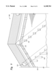
- FIGS. 4 and 5 are partial cross sectional views, detailing an embodiment of the faceplate 200 of the present invention.
- the faceplate 200 includes a top surface 210, a bottom surface 212, and a peripheral annular portion, or sidewall 214.
- a first gas pathway represented in this embodiment by the arrow A in FIG. 5, includes a first set of vertical channels 226, which extends through the faceplate 200 to provide fluid communication between an upper region 190, adjacent the top surface 210, and lower region 235, adjacent the bottom surface 212, where an upper limit of the upper region 190 is defined by the gas injection cover plate 110, shown in FIG. 3.
- a second gas pathway represented in this embodiment by the arrow B in FIG.
- the horizontal channels 222 form a labyrinth of channels in the faceplate 200 between the top surface 210 and the bottom surface 212.
- the horizontal channels 222 may be formed by machining, ie., drilling through the sidewall 214, in a plane generally parallel with the top surface 210 and bottom surface 212 of the faceplate. The incident angle of the drill bit determines the final configuration of the set of horizontal channels 222, while the bit size determines their diameter.
- a central gas inlet, or nozzle 224, disposed perpendicularly through the top surface 210 is in fluid communication with the horizontal channels 222 and is received by a lower portion of a conduit 184, shown in FIG. 3.
- An annular ring 230 adapted to circumferentially abut the sidewall 214, hermetically seals the endpoints of the set of horizontal channels 222. To help ensure an airtight seal, the ring 230 and the sidewall 214 may be fused together. Alternatively, the endpoints of the horizontal channels 222 may be individually plugged.
- FIG. 4 and 5 also show the second set of vertical channels 228, originating from the intersections of the set of horizontal channels 222 and offset from the first set of vertical channels 226.
- the second set of vertical channels 228 could originate from any point along the horizontal channels 222.
- the second set of vertical channels 228 is shown aligned with, or adjacent to, the first set of vertical channels 226.
- the faceplate 200 is preferably monolithic, i.e., machined or otherwise fabricated as a single piece of material, where the size and spacing of the holes may be varied according to the particular application, so that uniform delivery into the process chamber is achieved. Manufacturing the faceplate as a single piece of material avoids the problems encountered with aligning separate plates and preventing leakage of gases between plates and into separate channels.
- the gas feedthrough 108 mounts the gas injection plate 110, shown in FIG. 3 and comprises an inlet manifold 150, an outlet manifold 152, and a housing 154 interposed therebetween.
- a first gas tube 156 and a second gas tube 158 extend through the housing 154 to separately route two process gases therethrough.
- Two pairs of ports 159 are formed in the inlet manifold 150 and outlet manifold 152, respectively, to receive the first gas tube 156 and the second gas tube 158 at their respective ends.
- the gas tubes 156, 158 are shown as parallel to one another in FIG. 7, but may also be concentric, thereby coaxially delivering the gases separately into and through the gas feedthrough 108.
- the ports 159 formed in the inlet manifold 150 are aligned with gas delivery channels 162, 164 formed through the chamber body and the lid.
- the gas delivery channels 162, 164 are connected to the first supply line 120 and second supply line 122, respectively, at the bottom of the chamber body 101.
- a first container 116 and second container 118 are located upstream to supply the precursors to the gas distribution assembly 104 via a first supply line 120 and second supply line 122, respectively.
- Flow controllers 124 are disposed in the supply lines 120, 122 to regulate the flow rates of the precursors.
- a vaporizer 126 is disposed in the first supply line 120 to vaporize a liquid precursor, such as hydrogen peroxide.
- the gas feedthrough 108 provides for a first fluid feedthrough tube 168 and second fluid feedthrough tube 170 each connected to fluid delivery hoses 172 at a pair of quick-disconnect fittings 174, shown in FIG. 3.
- the fluid feedthrough tubes 168, 170 circulate a heat transfer fluid through an annular fluid passageway 180 formed in the gas injection cover plate 110 via coolant fluid inlet channel 176 and a coolant fluid outlet channel 178.
- the conduit 184 channels a second gas into the nozzle 224 which is received at a lower end of the conduit 184.
- the central bore 182 and the perimeter of the conduit 184 define a gas delivery passage 186, which delivers a gas above the blocker plate 112 and into the first set of vertical channels, shown in FIG. 3.
- the perforated blocker plate 112, suspended by screws 196, is horizontally disposed within the upper region 190.
- the blocker plate 112 is perpendicularly intersected by the gas conduit 184, which traverses the upper region 190 and terminates near the top surface 210, so that the conduit 184 and the top surface 210 are in mating abutment and hermetically sealed by an O-ring 198.
- FIG. 3 also shows a remote cooler 134 connected to the substrate support member 130 by coolant lines 135.
- a liquid coolant such as water, ethylene, glycol, or the like is delivered to the substrate support member 130, circulated through a spiraling cooling channel 137, and then circulated back to the cooler 134.
- the circulation of the fluid allows the temperature of the substrate support member 130 to be controlled.
- the substrate support member 130 is preferably made of aluminum, because of its excellent thermal conductive properties as well as its resistance to the corrosive effects of the chemical precursors.
- FIG. 3 shows a plurality of grooves 138 formed in the substrate seating surface 128. A substrate backside vacuum is achieved by attaching a vacuum pump 140 to the substrate support member 130 in communication with the grooves 138.
- the substrate 103 is positioned onto the substrate support member 130 by an external robot (not shown) through a slit valve aperture (also not shown) formed in the chamber body 101.
- a first gas is then supplied from the first gas container 116 and a second gas is supplied by the second gas container 118.
- the first and second gases are channeled through the chamber body 101 via gas delivery channels 162 and 164, respectively, and then flown through the gas feedthrough 108.
- the first gas is then routed through the gas delivery passage 186, while the second gas is routed through the delivery conduit 184.
- the first gas is delivered into the upper region 190, above the blocker plate 112, where the blocker plate 112 acts as an initial dispersion stage, forcing the first gas to pervade upper region 190 and diffuse over the upper surface of the blocker plate 112.
- the first gas then migrates through the perforations in the blocker plate 112, uniformly impinges on the top surface 210, and ultimately migrates through the first set of vertical channels 226 into the process region 102 as shown by pathway arrows A in FIG. 5.
- the second gas is channeled through the nozzle 224, and is diffused throughout the second gas pathway 216, shown in FIG. 5, including the set of interconnected horizontal channels 222.
- the second gas then flows through the second set of vertical channels 228 into the process region 102, where it reacts with the first gas.
- the pathway of the second gas is shown in FIG. 5 by arrows B.
- the precursors used and the particular chamber conditions applied, such as temperature and pressure, depend on the desired reaction and film composition.
- the chamber 100 is particularly suited for plasma-less condensation reactions, such as between methylsilane and hydrogen peroxide, wherein the reactants are not mixed prior to entering the processing region 102 and the substrate 103 is preferably maintained at a low temperature.
- the particular deposition process involving methylsilane and hydrogen peroxide is preferably performed while maintaining the substrate 103 between about -20° C. to 25° C.
- FIGS. 8 and 9 illustrate an alternative embodiment of the faceplate 200.
- This embodiment applies a multi-tiered approach, whereby a first set of horizontal channels of a first gas pathway is vertically offset from a second set of horizontal channels of a second gas pathway.
- the faceplate 200 is shown, having a first set of horizontal channels 314 coplanar with a second set of horizontal channels 316.
- a centrally located first gas supply pipe 318 delivers a first gas to the first set of horizontal channels 314, while a coaxial second gas supply pipe 320 delivers a second gas to the second set of horizontal channels 316.
- a first set of vertical channels 322 is formed through a lower surface 324 to provide for fluid flow from the first set of horizontal channels 314 to a region below the faceplate 200.
- a second set of vertical channels 326 is formed in the lower surface 324 to provide fluid flow from the second set of horizontal channels 316 to the region below the faceplate 200.
- FIG. 8 shows a bottom view of faceplate 200 with the horizontal channels 314, 316 radially extending from a central hub 328, or cavity, wherein the horizontal channels 314, 316 originate.
- the channels 314, 316 may take on the design of the interconnecting horizontal channels 222 shown in FIGS. 5-6 or other designs, as the marketplace and manufacturing concerns direct.
- the multi-tiered concept of FIGS. 8 and 9 may be extrapolated to devise a faceplate capable of separately delivering three or more gases simply by adding additional tiers of horizontal channels, each communicating with separate vertical channels.
- the latter embodiment has the added advantage of dispensing with the need for a blocker plate 112, shown in FIG. 3. Because the reactant gases are delivered directly to the radial horizontal channels 314, 316 by pipes 318 and 320, a blocker plate is unnecessary.
- the chamber 100 of FIG. 3 may be modified so that the first gas supply pipe 318 and second gas supply pipe 320 are connected directly to the manifold ports 159, formed in the inlet manifold 150, shown in FIG. 6.
- FIGS. 10 and 11 show additional embodiments of the present invention.
- FIG. 10 shows a plurality of nozzles 330 (three shown) equally spaced around a central portion of the faceplate 200.
- FIG. 11 shows the nozzles 330 disposed around the perimeter portion of the faceplate 200. Although only two patterns are shown here, a person skilled in the art will recognize additional geometric configurations.
- FIG. 12 is a perspective view of an alternative embodiment of a gas delivery system of the invention.
- a multi-pronged manifold 332 is provided to deliver a gas from a central feed to the outer portion of the gas faceplate.
- a manifold inlet 334 is then mounted to the conduit 184 similar to the nozzle 224, described above in reference to FIG. 5.
- a plurality of manifold outlet conduits 336 are coupled to the nozzles to deliver a gas into the second gas pathway 216, shown in FIG. 5.
- the first gas is flown through the first set of vertical channels 226 and into the processing region 102, shown in FIG. 3.
- the second gas is flown into the manifold inlet 334.
- the second gas is then delivered into the second gas pathway 216 of the faceplate 200 by the set of manifold outlet conduits 336 and uniformly delivered to the process region 102 via the second set of vertical channels 228, shown in FIG. 5.
- the present invention is particularly suited for forming SiO 2 films by reacting methlysilane with hydrogen peroxide.
- the methlysilane and the hydrogen peroxide are delivered separately into the processing chamber.
- the process steps of the reaction are believed to be as follows: ##STR1##
- Step 1 is performed on a cold substrate, preferably between about -20° C. to 25° C., to yield a silanol-type compound.
- Step 2 describes a condensation reaction wherein a conformal porous SiO 2 network is achieved. The substrate is then heated to dehydrate the films and form a porous oxide.
Abstract
A multi-channel faceplate 200, that in some embodiments is monolithic, is provided as a portion of a gas delivery system to a process chamber 100. At least two sets of gas pathways are disposed through a faceplate and allow for independent delivery of separate gases into a process chamber 100. In one embodiment, a first gas pathway, which includes a first set of vertical channels 226, is formed through the faceplate 200. A second gas pathway includes a second set of vertical channels 228, which is formed through a portion of the faceplate and connected to a set of interconnecting horizontal channels 222 in the faceplate 200, where the second gas pathway maintains fluidic separation from the first gas pathway, prior to the gases entering the process chamber 100.
Description
This application claims priority of U.S. Provisional Patent Application Serial No. 60/089,413, filed Jun. 16, 1998.
1. Field of the Invention
The present invention generally relates to the field of semiconductor substrate processing equipment. More particularly, the present invention relates to a gas distribution system which provides separate and uniform delivery of two or more gases into a processing chamber.
2. Background of Related Art
In the fabrication of integrated circuits, vacuum process chambers are generally employed to process semiconductor substrates. The processes carried out in the vacuum chambers typically provide the deposition or etching of multiple metal, dielectric, and semiconductor layers on the surface of a substrate. Examples of such processes include chemical vapor deposition (CVD), physical vapor deposition (PVD), and etching processes. Many processing chambers include a gas distribution system to effectuate depositions, etching, and so forth. Dry etching of semiconductor materials can also be conducted with chemical vapor transport systems to selectively remove desired areas of such materials to form a desired pattern or configuration on a substrate.
To better understand the integration of a gas distributing system in a processing chamber, FIG. 1 is a schematic diagram showing the construction of a typical CVD chamber 10. The chamber 10 generally defines a processing region 12 and houses a vertically movable substrate support member 14. Containers 20 are provided to supply a variety of gases needed to carry out the processes in the chamber 10. A vaporizer 22 is provided to heat and vaporize one or more liquid precursors, while a flow controller 24 governs the rate at which gases are delivered into the chamber 10. For processes requiring multiple gases, the chamber 10 typically includes an upstream premixing chamber 26, wherein process gases are combined prior to being introduced into the processing region 12.
Gas delivery into the chamber 10 is accomplished by a gas distribution assembly 28, shown in detail in FIG. 2, consisting of a gas manifold 30, a gas box 32 (or gas injection cover plate), a showerhead assembly 34, and an isolator 36, all of which are mounted on an electrically grounded chamber lid 38. The showerhead 34 typically comprises a perforated blocker plate 40 and a faceplate 42 having an array of holes 44. Both the blocker plate 40 and the faceplate 42 are generally flat circular members through which gases are diffused or passed to provide a uniform concentration of gases over the substrate surface. A cavity between the blocker plate 40 and the gas box 32 also serves as an additional agitation stage to continue mixing the process gases. O-rings 46 are disposed between the various components to help ensure hermitic seals to prevent leakage of the gases. In operation, the process gases are pumped into the CVD chamber 10 to effectuate deposition onto a substrate.
Improvements in gas distribution systems are needed, because as integrated circuit density increases and feature size decreases, new materials having low dielectric constants in plasma-less deposition are being developed. In the area of dielectrics, for example, silicon dioxide (SiO2) is formed by mixing methylsilane (SiH3 CH3) and hydrogen peroxide (H2 O2). These chemicals undergo a condensation reaction on a cooled substrate to form a porous oxide network.
Critical to the use of H2 O2 and SiH3 CH3 is keeping the chemicals separate during delivery into the chamber to prevent them from reacting prior to their introduction into a processing region of a vacuum chamber. Allowing a reaction to occur at any point upstream of the processing region results in clogging of equipment components, such as the faceplate 42 and blocker plate 40 of a vacuum chamber gas distribution assembly. Once the gas distribution plates are obstructed, the gases no longer uniformly distribute across the surface of the substrate and nonconformal deposition patterns can result, thereby producing defective devices. In order to clean the gas distribution plates, production must be interrupted and the gas delivery system must be disassembled, serviced, and reassembled.
One attempt to provide a dual channel delivery showerhead is shown in U.S. Pat. No. 5,624,494 entitled "Showerhead for a Gas Supplying Apparatus." The showerhead arrangement disclosed includes two separate perforated plates, each providing a separate gas pathway, joined at an interface. A first set of holes is formed in both a top plate and a bottom plate and must be aligned when the plates are assembled to form a continuous channel through both plates. A second pathway is defined by a third set of vertical holes formed in the bottom plate and fluidly connected by a set of horizontal recesses also formed in the bottom plate. Concentric gas pipes separately deliver reactive gases to the first and second pathways, which then route the gases into a process chamber for mixing and deposition on to a substrate.
One difficulty encountered with this gas plate is achieving the alignment of the holes formed within the two perforated plates. This alignment is critical and is difficult to achieve. Another problem is ensuring a gas-tight seal between the plates to prevent leakage between the holes. As a consequence, the reactive gases migrate through the interstitial spaces formed between the plates and holes and deposit thereon. For processes involving reactive gases, such as H2 O2 and SiH3 CH3, the resulting chemical compound clogs the gas delivery system and ultimately leads to a non-uniform deposition pattern on the substrates. Furthermore, the blockage requires, at a minimum, cleaning of the showerhead. Substantial blockage may also use upstream pumping equipment and require their maintenance or replacement.
A need, therefore, exists for a gas distribution assembly which provides for separate introduction of gases into a process chamber which uniformly delivers gases onto a substrate without the above blockage problems.
The present invention generally provides a substrate processing chamber, apparatus, and associated methods, having a gas distribution system that provides separate and uniform distribution of two or more gases within the processing chamber. In one embodiment, the invention provides an apparatus for distributing gases within a processing chamber comprising a monolithic multi-channel faceplate. A first gas pathway, having a first set of vertical channels, extends through the faceplate. A second gas pathway, having a second set of vertical channels intersecting a set of horizontal channels, is separated from the first gas pathway through the monolithic faceplate. Separate gas supplies deliver gases to each of the gas pathways. This faceplate may be particularly useful in a plasma-less processing chamber. The faceplate separately delivers reactive gases into a processing region, which are mixed following delivery into the processing region and deposited on a substrate, which may be supported on a temperature-controlled support member. Naturally, other embodiments are possible.
In one embodiment, the present invention includes an apparatus for distributing gas in a processing system, comprising a monolithic multi-channel faceplate adapted to disperse gases into a process chamber, a first gas pathway through the monolithic multi-channel faceplate adapted to deliver a first gas to the process chamber, and at least a second gas pathway through the monolithic multi-channel faceplate, the second gas pathway adapted to deliver at least a second gas to the process chamber substantially separate from the first gas prior to delivery to the process chamber. In another embodiment, the present invention includes an apparatus for distributing gas in a processing system, comprising a multi-channel faceplate adapted to disperse gases into a process chamber, a first gas pathway through the faceplate comprising a first set of horizontal channels intersecting a first set of vertical channels for a first gas, at least a second gas pathway through the faceplate comprising a second set of horizontal channels disposed vertically offset with respect to the first set of horizontal channels and intersecting a second set of vertical channels separate from the first set of vertical channels. In yet another embodiment, the present invention includes a semiconductor processing apparatus, comprising a process chamber and a gas distribution system connected to the process chamber, the gas distribution system comprising a gas feedthrough fluidicly connected to a first and second gas source, a gas injection cover plate fluidicly connected on an upper side to the gas feedthrough, and a monolithic multi-channel faceplate connected to a lower side of the gas injection cover plate, the faceplate adapted for the separate delivery to the process chamber of two or more gases.
So that the manner in which the above recited features, advantages and objects of the present invention are attained and can be understood in detail, a more particular description of the invention, briefly summarized above, may be had by reference to the embodiments thereof which are illustrated in the appended drawings.
It is to be noted, however, that the appended drawings illustrate only typical embodiments of this invention and are therefore not to be considered limiting of its scope, for the invention may admit to other equally effective embodiments.
FIG. 1 is a schematic diagram of a prior art CVD chamber;
FIG. 2 is an exploded diagram, depicting the components of a prior art gas distribution system;
FIG. 3 is a partial cross sectional view of a process chamber;
FIG. 4 is a partial cross sectional view of one embodiment of a monolithic multi-channeled faceplate of the present invention;
FIG. 5 is an enlarged partial cross sectional view of the faceplate of FIG. 4, having offset vertical channels;
FIG. 6 is an enlarged partial cross sectional view showing a second embodiment of the present invention, having aligned vertical channels;
FIG. 7 is an exploded sectional view of a gas feedthrough in a vertical orientation;
FIG. 8 is a bottom view of another embodiment of the present invention, having multiple horizontal layers vertically offset from each other;
FIG. 9 is a partial cross sectional perspective view of the embodiment shown in FIG. 8;
FIG. 10 is perspective view of another embodiment of the present invention, having separate nozzles;
FIG. 11 is perspective view of another embodiment of the present invention, having separate nozzles disposed about the periphery of the faceplate;
FIG. 12 is perspective view of another embodiment of the present invention, having a multi-pronged manifold.
The present invention generally provides a substrate processing chamber having a gas distribution system that provides separate and uniform distribution of two or more gases within the processing chamber. The present invention includes a semiconductor processing apparatus, having a process chamber and a gas distribution system connected to the process chamber, the gas distribution system including a gas feedthrough fluidicly connected to a first and second gas source, a gas injection cover plate fluidicly connected on an upper side to the gas feedthrough and a monolithic multi-channel faceplate connected to a lower side of the gas injection cover plate, the faceplate adapted for the separate delivery to the process chamber of two or more gases. A first gas pathway, having a first set of vertical channels, extends through the faceplate. A second gas pathway, having a second set of vertical channels intersecting a set of horizontal channels, is separated from the first gas pathway through the monolithic faceplate. Separate gas supplies deliver gases to each of the gas pathways. Naturally, other embodiments are possible.
FIG. 3 shows a cross sectional view of one embodiment of a processing chamber 100, incorporating the present invention. The chamber 100 generally includes a chamber body 101, enclosing a processing region 102, wherein chemical precursors are introduced during processing. A vertically movable temperature-controlled substrate support member 130 is disposed through a lower end of the chamber body 101 to support a substrate thereon. The substrate support member 130 includes a cooling channel 137, through which a fluid is passed to effect heating and/or cooling of the support member 130. An annular vacuum exhaust channel 132, connected to a vacuum pump 129, is provided to expel process gases from the processing region 102. A top gas distribution assembly 104 is disposed on a lid 106 to deliver gases into the chamber 100. The gas distribution assembly 104 comprises a gas feedthrough 108, a gas injection cover plate 110, a blocker plate 112, and a multi-channel faceplate 200. The faceplate 200 is shown incorporated into the chamber 100 as part of the gas distribution assembly 104, so that the faceplate 200 defines the upper limit of the processing region 102. The lid 106 mounts the faceplate 200 and supports the gas injection cover plate 110. O-rings 195, located in the flange 194, provide a seal between the flange 194 of the faceplate 200 and the lid 106. A cover 148 is disposed over the lid 106. The faceplate 200, described in detail below, is uniquely designed to separately deliver a first and a second precursor gas into the processing region 102 via gas channels. In general, the channels comprise a set of vertical and horizontal channels formed in the faceplate 200.
FIGS. 4 and 5 are partial cross sectional views, detailing an embodiment of the faceplate 200 of the present invention. The faceplate 200 includes a top surface 210, a bottom surface 212, and a peripheral annular portion, or sidewall 214. A first gas pathway, represented in this embodiment by the arrow A in FIG. 5, includes a first set of vertical channels 226, which extends through the faceplate 200 to provide fluid communication between an upper region 190, adjacent the top surface 210, and lower region 235, adjacent the bottom surface 212, where an upper limit of the upper region 190 is defined by the gas injection cover plate 110, shown in FIG. 3. A second gas pathway, represented in this embodiment by the arrow B in FIG. 5, includes a second set of vertical channels 228, which extends through the bottom surface 212 and provide fluid communication between a set of horizontal channels 222 and the lower region 235. The horizontal channels 222 form a labyrinth of channels in the faceplate 200 between the top surface 210 and the bottom surface 212. The horizontal channels 222 may be formed by machining, ie., drilling through the sidewall 214, in a plane generally parallel with the top surface 210 and bottom surface 212 of the faceplate. The incident angle of the drill bit determines the final configuration of the set of horizontal channels 222, while the bit size determines their diameter. A central gas inlet, or nozzle 224, disposed perpendicularly through the top surface 210 is in fluid communication with the horizontal channels 222 and is received by a lower portion of a conduit 184, shown in FIG. 3. An annular ring 230, adapted to circumferentially abut the sidewall 214, hermetically seals the endpoints of the set of horizontal channels 222. To help ensure an airtight seal, the ring 230 and the sidewall 214 may be fused together. Alternatively, the endpoints of the horizontal channels 222 may be individually plugged.
FIG. 4 and 5 also show the second set of vertical channels 228, originating from the intersections of the set of horizontal channels 222 and offset from the first set of vertical channels 226. However, the second set of vertical channels 228 could originate from any point along the horizontal channels 222. For example, as shown in FIG. 6, the second set of vertical channels 228 is shown aligned with, or adjacent to, the first set of vertical channels 226.
The faceplate 200 is preferably monolithic, i.e., machined or otherwise fabricated as a single piece of material, where the size and spacing of the holes may be varied according to the particular application, so that uniform delivery into the process chamber is achieved. Manufacturing the faceplate as a single piece of material avoids the problems encountered with aligning separate plates and preventing leakage of gases between plates and into separate channels.
The gas feedthrough 108, shown in a vertical exploded sectional view in FIG. 7, mounts the gas injection plate 110, shown in FIG. 3 and comprises an inlet manifold 150, an outlet manifold 152, and a housing 154 interposed therebetween. A first gas tube 156 and a second gas tube 158 extend through the housing 154 to separately route two process gases therethrough. Two pairs of ports 159 are formed in the inlet manifold 150 and outlet manifold 152, respectively, to receive the first gas tube 156 and the second gas tube 158 at their respective ends. The gas tubes 156, 158 are shown as parallel to one another in FIG. 7, but may also be concentric, thereby coaxially delivering the gases separately into and through the gas feedthrough 108. The ports 159 formed in the inlet manifold 150 are aligned with gas delivery channels 162, 164 formed through the chamber body and the lid. The gas delivery channels 162, 164 are connected to the first supply line 120 and second supply line 122, respectively, at the bottom of the chamber body 101. A first container 116 and second container 118 are located upstream to supply the precursors to the gas distribution assembly 104 via a first supply line 120 and second supply line 122, respectively. Flow controllers 124 are disposed in the supply lines 120, 122 to regulate the flow rates of the precursors. A vaporizer 126 is disposed in the first supply line 120 to vaporize a liquid precursor, such as hydrogen peroxide.
The gas feedthrough 108 provides for a first fluid feedthrough tube 168 and second fluid feedthrough tube 170 each connected to fluid delivery hoses 172 at a pair of quick-disconnect fittings 174, shown in FIG. 3. The fluid feedthrough tubes 168, 170 circulate a heat transfer fluid through an annular fluid passageway 180 formed in the gas injection cover plate 110 via coolant fluid inlet channel 176 and a coolant fluid outlet channel 178.
A central bore 182, shown in FIG. 3, disposed through the gas injection cover plate 110, houses a coaxially disposed gas conduit 184, which delivers a gas to second gas pathway 216, shown in FIGS. 5 and 6 which includes the second set of horizontal channels 222. The conduit 184 channels a second gas into the nozzle 224 which is received at a lower end of the conduit 184. The central bore 182 and the perimeter of the conduit 184 define a gas delivery passage 186, which delivers a gas above the blocker plate 112 and into the first set of vertical channels, shown in FIG. 3. The perforated blocker plate 112, suspended by screws 196, is horizontally disposed within the upper region 190. The blocker plate 112 is perpendicularly intersected by the gas conduit 184, which traverses the upper region 190 and terminates near the top surface 210, so that the conduit 184 and the top surface 210 are in mating abutment and hermetically sealed by an O-ring 198.
FIG. 3 also shows a remote cooler 134 connected to the substrate support member 130 by coolant lines 135. A liquid coolant such as water, ethylene, glycol, or the like is delivered to the substrate support member 130, circulated through a spiraling cooling channel 137, and then circulated back to the cooler 134. The circulation of the fluid allows the temperature of the substrate support member 130 to be controlled. To ensure a highly efficient heat exchange, the substrate support member 130 is preferably made of aluminum, because of its excellent thermal conductive properties as well as its resistance to the corrosive effects of the chemical precursors. FIG. 3 shows a plurality of grooves 138 formed in the substrate seating surface 128. A substrate backside vacuum is achieved by attaching a vacuum pump 140 to the substrate support member 130 in communication with the grooves 138.
In operation, the substrate 103 is positioned onto the substrate support member 130 by an external robot (not shown) through a slit valve aperture (also not shown) formed in the chamber body 101. A first gas is then supplied from the first gas container 116 and a second gas is supplied by the second gas container 118. The first and second gases are channeled through the chamber body 101 via gas delivery channels 162 and 164, respectively, and then flown through the gas feedthrough 108. The first gas is then routed through the gas delivery passage 186, while the second gas is routed through the delivery conduit 184. The first gas is delivered into the upper region 190, above the blocker plate 112, where the blocker plate 112 acts as an initial dispersion stage, forcing the first gas to pervade upper region 190 and diffuse over the upper surface of the blocker plate 112. The first gas then migrates through the perforations in the blocker plate 112, uniformly impinges on the top surface 210, and ultimately migrates through the first set of vertical channels 226 into the process region 102 as shown by pathway arrows A in FIG. 5. Simultaneously, the second gas is channeled through the nozzle 224, and is diffused throughout the second gas pathway 216, shown in FIG. 5, including the set of interconnected horizontal channels 222. The second gas then flows through the second set of vertical channels 228 into the process region 102, where it reacts with the first gas. The pathway of the second gas is shown in FIG. 5 by arrows B.
The precursors used and the particular chamber conditions applied, such as temperature and pressure, depend on the desired reaction and film composition. However, the chamber 100 is particularly suited for plasma-less condensation reactions, such as between methylsilane and hydrogen peroxide, wherein the reactants are not mixed prior to entering the processing region 102 and the substrate 103 is preferably maintained at a low temperature. The particular deposition process involving methylsilane and hydrogen peroxide is preferably performed while maintaining the substrate 103 between about -20° C. to 25° C.
FIGS. 8 and 9 illustrate an alternative embodiment of the faceplate 200. This embodiment applies a multi-tiered approach, whereby a first set of horizontal channels of a first gas pathway is vertically offset from a second set of horizontal channels of a second gas pathway. The faceplate 200 is shown, having a first set of horizontal channels 314 coplanar with a second set of horizontal channels 316. A centrally located first gas supply pipe 318 delivers a first gas to the first set of horizontal channels 314, while a coaxial second gas supply pipe 320 delivers a second gas to the second set of horizontal channels 316. A first set of vertical channels 322 is formed through a lower surface 324 to provide for fluid flow from the first set of horizontal channels 314 to a region below the faceplate 200. Similarly, a second set of vertical channels 326 is formed in the lower surface 324 to provide fluid flow from the second set of horizontal channels 316 to the region below the faceplate 200.
FIG. 8 shows a bottom view of faceplate 200 with the horizontal channels 314, 316 radially extending from a central hub 328, or cavity, wherein the horizontal channels 314, 316 originate. However, the channels 314, 316 may take on the design of the interconnecting horizontal channels 222 shown in FIGS. 5-6 or other designs, as the marketplace and manufacturing concerns direct. Furthermore, the multi-tiered concept of FIGS. 8 and 9 may be extrapolated to devise a faceplate capable of separately delivering three or more gases simply by adding additional tiers of horizontal channels, each communicating with separate vertical channels.
The latter embodiment has the added advantage of dispensing with the need for a blocker plate 112, shown in FIG. 3. Because the reactant gases are delivered directly to the radial horizontal channels 314, 316 by pipes 318 and 320, a blocker plate is unnecessary. Thus, the chamber 100 of FIG. 3 may be modified so that the first gas supply pipe 318 and second gas supply pipe 320 are connected directly to the manifold ports 159, formed in the inlet manifold 150, shown in FIG. 6.
FIGS. 10 and 11 show additional embodiments of the present invention. FIG. 10 shows a plurality of nozzles 330 (three shown) equally spaced around a central portion of the faceplate 200. Alternatively, FIG. 11 shows the nozzles 330 disposed around the perimeter portion of the faceplate 200. Although only two patterns are shown here, a person skilled in the art will recognize additional geometric configurations.
FIG. 12 is a perspective view of an alternative embodiment of a gas delivery system of the invention. A multi-pronged manifold 332 is provided to deliver a gas from a central feed to the outer portion of the gas faceplate. A manifold inlet 334 is then mounted to the conduit 184 similar to the nozzle 224, described above in reference to FIG. 5. A plurality of manifold outlet conduits 336 are coupled to the nozzles to deliver a gas into the second gas pathway 216, shown in FIG. 5. In operation, the first gas is flown through the first set of vertical channels 226 and into the processing region 102, shown in FIG. 3. Simultaneously, the second gas is flown into the manifold inlet 334. The second gas is then delivered into the second gas pathway 216 of the faceplate 200 by the set of manifold outlet conduits 336 and uniformly delivered to the process region 102 via the second set of vertical channels 228, shown in FIG. 5.
As noted above, the present invention is particularly suited for forming SiO2 films by reacting methlysilane with hydrogen peroxide. The methlysilane and the hydrogen peroxide are delivered separately into the processing chamber. The process steps of the reaction are believed to be as follows: ##STR1##
Step 1 is performed on a cold substrate, preferably between about -20° C. to 25° C., to yield a silanol-type compound. Step 2 describes a condensation reaction wherein a conformal porous SiO2 network is achieved. The substrate is then heated to dehydrate the films and form a porous oxide.
While the foregoing is directed to a preferred embodiment of the invention, other and further embodiments of the invention may be devised without departing from the basic scope of thereof, and the scope thereof is determined by the claims which follow.
Claims (19)
1. An apparatus for distributing gas in a processing system, comprising:
a) a monolithic multi-channel faceplate adapted to disperse gases into a process chamber;
b) a first gas pathway disposed through the monolithic multi-channel faceplate adapted to deliver a first gas to the process chamber; and
c) at least a second gas pathway disposed through the monolithic multi-channel faceplate, the second gas pathway adapted to deliver at least a second gas to the process chamber substantially separate from the first gas prior to delivery to the process chamber.
2. The apparatus of claim 1, wherein the first gas pathway comprises a first set of vertical channels and the second gas pathway comprises a set of horizontal channels intersecting a second set of vertical channels separate from the first set of vertical channels.
3. The apparatus of claim 1, further comprising a first manifold upstream from the multi-channel faceplate to deliver the first gas to the faceplate and a second gas conduit separate from the first manifold to deliver the second gas to the second gas pathway.
4. The apparatus of claim 3, wherein at least a portion of the first manifold is coaxial with the second gas conduit to the second gas pathway.
5. The apparatus of claim 2, wherein the second set of vertical channels perpendicularly intersects the horizontal channels.
6. The apparatus of claim 2, wherein the first set of vertical channels is aligned with the second set of vertical channels.
7. The apparatus of claim 2, wherein the first set of vertical channels is offset from the second set of vertical channels.
8. The apparatus of claim 1, further comprising a first set of horizontal channels intersecting a first set of vertical channels for the first gas pathway and a second set of horizontal channels disposed vertically offset from the first set of horizontal channels and intersecting a second set of vertical channels separate from the first set of vertical channels for the second gas pathway.
9. The apparatus of claim 1, further comprising a plurality of separate nozzles fluidly connected to the second gas pathway adapted to deliver the second gas to the second gas pathway.
10. The apparatus of claim 1, further comprising a central feed fluidicly connected to a multi-pronged manifold wherein the multi-pronged manifold is fluidly connected to a plurality of separate nozzles adapted to deliver the second gas to the second gas pathway.
11. The apparatus of claim 1, further comprising a seal disposed about the periphery of the faceplate to seal the horizontal channels extending to the periphery.
12. An apparatus for distributing gas in a processing system, comprising:
a) a multi-channel faceplate adapted to disperse gases into a process chamber;
b) a first gas pathway through the faceplate comprising a first set of horizontal channels intersecting a first set of vertical channels for a first gas; and
c) at least a second gas pathway through the faceplate comprising a second set of horizontal channels disposed vertically offset from the first set of horizontal channels and intersecting a second set of vertical channels separate from the first set of vertical channels.
13. The apparatus of claim 12, further comprising a plurality of separate nozzles fluidly connected to the second gas pathway and adapted to deliver the second gas to the second gas pathway.
14. A semiconductor processing apparatus, comprising:
(a) a process chamber; and
(b) a gas distribution system connected to the process chamber, the gas distribution system comprising:
(i) a gas feedthrough fluidicly connected to a first and second gas source;
(ii) a gas injection cover plate fluidicly connected to the gas feedthrough; and
(iii) a monolithic multi-channel faceplate connected to the gas injection cover plate, the faceplate adapted for the separate delivery to the process chamber of two or more gases.
15. An apparatus for distributing gas in a processing system, comprising:
a) a monolithic multi-channel faceplate;
b) a first gas pathway having a first set of vertical channels disposed through the monolithic multi-channel faceplate; and
c) at least a second gas pathway disposed through the monolithic multi-channel faceplate, the second gas pathway having a set of horizontal channels intersecting a second set of vertical channels separate from the first set of vertical channels.
16. The apparatus of claim 15, further comprising a first manifold disposed upstream from the multi-channel faceplate and a second gas conduit separate from the first manifold.
17. The apparatus of claim 15, wherein the second set of vertical channels perpendicularly intersect the horizontal channels.
18. The apparatus of claim 15, wherein the first set of vertical channels is aligned with the second set of vertical channels.
19. The apparatus of claim 15, wherein the first set of vertical channels is offset from the second set of vertical channels.
Priority Applications (7)
| Application Number | Priority Date | Filing Date | Title |
|---|---|---|---|
| US09/207,780 US6148761A (en) | 1998-06-16 | 1998-12-09 | Dual channel gas distribution plate |
| TW088109311A TW552312B (en) | 1998-06-16 | 1999-06-04 | Dual channel gas distribution plate |
| DE69903466T DE69903466T2 (en) | 1998-06-16 | 1999-06-08 | GAS DISTRIBUTION PLATE WITH TWO GAS CHANNELS |
| PCT/US1999/012854 WO1999066101A1 (en) | 1998-06-16 | 1999-06-08 | Dual channel gas distribution plate |
| JP2000554902A JP4564656B2 (en) | 1998-06-16 | 1999-06-08 | Dual channel gas distribution plate |
| EP99928470A EP1129234B1 (en) | 1998-06-16 | 1999-06-08 | Dual channel gas distribution plate |
| KR1020007014255A KR100687373B1 (en) | 1998-06-16 | 1999-06-08 | Apparatus for distributing gas |
Applications Claiming Priority (2)
| Application Number | Priority Date | Filing Date | Title |
|---|---|---|---|
| US8941398P | 1998-06-16 | 1998-06-16 | |
| US09/207,780 US6148761A (en) | 1998-06-16 | 1998-12-09 | Dual channel gas distribution plate |
Publications (1)
| Publication Number | Publication Date |
|---|---|
| US6148761A true US6148761A (en) | 2000-11-21 |
Family
ID=26780566
Family Applications (1)
| Application Number | Title | Priority Date | Filing Date |
|---|---|---|---|
| US09/207,780 Expired - Lifetime US6148761A (en) | 1998-06-16 | 1998-12-09 | Dual channel gas distribution plate |
Country Status (7)
| Country | Link |
|---|---|
| US (1) | US6148761A (en) |
| EP (1) | EP1129234B1 (en) |
| JP (1) | JP4564656B2 (en) |
| KR (1) | KR100687373B1 (en) |
| DE (1) | DE69903466T2 (en) |
| TW (1) | TW552312B (en) |
| WO (1) | WO1999066101A1 (en) |
Cited By (470)
| Publication number | Priority date | Publication date | Assignee | Title |
|---|---|---|---|---|
| US6559424B2 (en) | 2001-01-02 | 2003-05-06 | Mattson Technology, Inc. | Windows used in thermal processing chambers |
| EP1361604A1 (en) * | 2001-01-22 | 2003-11-12 | Tokyo Electron Limited | Device and method for treatment |
| US20040050492A1 (en) * | 2002-09-16 | 2004-03-18 | Applied Materials, Inc. | Heated gas distribution plate for a processing chamber |
| US20040052969A1 (en) * | 2002-09-16 | 2004-03-18 | Applied Materials, Inc. | Methods for operating a chemical vapor deposition chamber using a heated gas distribution plate |
| US20040076763A1 (en) * | 2002-09-20 | 2004-04-22 | Hiroya Kirimura | Apparatus and method for forming a thin flim |
| US20040142558A1 (en) * | 2002-12-05 | 2004-07-22 | Granneman Ernst H. A. | Apparatus and method for atomic layer deposition on substrates |
| US20040216665A1 (en) * | 2003-04-29 | 2004-11-04 | Asm International N.V. | Method and apparatus for depositing thin films on a surface |
| US20040216668A1 (en) * | 2003-04-29 | 2004-11-04 | Sven Lindfors | Showerhead assembly and ALD methods |
| US6818096B2 (en) * | 2001-04-12 | 2004-11-16 | Michael Barnes | Plasma reactor electrode |
| US20040250763A1 (en) * | 2002-01-11 | 2004-12-16 | Ovshinsky Stanford R. | Fountain cathode for large area plasma deposition |
| US20050217580A1 (en) * | 2003-05-30 | 2005-10-06 | Aviza Technology, Inc. | Gas distribution system |
| US20060090850A1 (en) * | 2003-03-26 | 2006-05-04 | Tokyo Electron Limited | Chemical processing system and method |
| US20060124061A1 (en) * | 2004-12-13 | 2006-06-15 | Tateo Saito | Molecule supply source for use in thin-film forming |
| US20060162661A1 (en) * | 2005-01-22 | 2006-07-27 | Applied Materials, Inc. | Mixing energized and non-energized gases for silicon nitride deposition |
| US20070022959A1 (en) * | 2005-07-29 | 2007-02-01 | Craig Bercaw | Deposition apparatus for semiconductor processing |
| US20070151516A1 (en) * | 2006-01-03 | 2007-07-05 | Law Kam S | Chemical vapor deposition apparatus and electrode plate thereof |
| US20070264427A1 (en) * | 2005-12-21 | 2007-11-15 | Asm Japan K.K. | Thin film formation by atomic layer growth and chemical vapor deposition |
| US20070272154A1 (en) * | 2003-10-23 | 2007-11-29 | Manabu Amikura | Shower Head and Film-Forming Device Using the Same |
| US20070281106A1 (en) * | 2006-05-30 | 2007-12-06 | Applied Materials, Inc. | Process chamber for dielectric gapfill |
| US20080092815A1 (en) * | 2006-10-18 | 2008-04-24 | Advanced Micro-Fabrication Equipment, Inc. Asia | Gas distribution assembly for use in a semiconductor work piece processing reactor |
| US20080099147A1 (en) * | 2006-10-26 | 2008-05-01 | Nyi Oo Myo | Temperature controlled multi-gas distribution assembly |
| US20090095222A1 (en) * | 2007-10-16 | 2009-04-16 | Alexander Tam | Multi-gas spiral channel showerhead |
| US20090107403A1 (en) * | 2007-10-31 | 2009-04-30 | Moshtagh Vahid S | Brazed cvd shower head |
| US20090120368A1 (en) * | 2007-11-08 | 2009-05-14 | Applied Materials, Inc. | Rotating temperature controlled substrate pedestal for film uniformity |
| US20090163001A1 (en) * | 2007-12-21 | 2009-06-25 | Asm America, Inc. | Separate injection of reactive species in selective formation of films |
| US20090255912A1 (en) * | 2008-04-09 | 2009-10-15 | The Boeing Company | Purge and sealant cap for selective laser sintering build frame |
| US7718004B2 (en) | 2004-10-29 | 2010-05-18 | Asm Japan K.K. | Gas-introducing system and plasma CVD apparatus |
| US20100126418A1 (en) * | 2008-11-26 | 2010-05-27 | Industrial Technology Research Institute | Gas shower module |
| US20100303674A1 (en) * | 2009-05-31 | 2010-12-02 | James Scott Sutherland | Reactor With Upper and Lower Manifold Structures |
| US20100307415A1 (en) * | 2009-04-06 | 2010-12-09 | Eric Shero | Semiconductor processing reactor and components thereof |
| US7893433B2 (en) | 2001-02-12 | 2011-02-22 | Asm America, Inc. | Thin films and methods of making them |
| US20110073038A1 (en) * | 2009-09-25 | 2011-03-31 | Industrial Technology Research Institute | Gas distribution plate and apparatus using the same |
| US7939447B2 (en) | 2007-10-26 | 2011-05-10 | Asm America, Inc. | Inhibitors for selective deposition of silicon containing films |
| US20110308456A1 (en) * | 2010-06-21 | 2011-12-22 | Hon Hai Precision Industry Co., Ltd. | Coating apparatus |
| US20120100311A1 (en) * | 2009-08-28 | 2012-04-26 | Kyocera Corporation | Apparatus for forming deposited film and method for forming deposited film |
| US8486191B2 (en) | 2009-04-07 | 2013-07-16 | Asm America, Inc. | Substrate reactor with adjustable injectors for mixing gases within reaction chamber |
| US20130220222A1 (en) * | 2012-02-23 | 2013-08-29 | Hermes-Epitek Corporation | Gas Distribution Apparatus with Heat Exchanging Channels |
| US20130341433A1 (en) * | 2012-06-22 | 2013-12-26 | Shambhu N. Roy | Dual plenum, axi-symmetric showerhead with edge-to-center gas delivery |
| US8728832B2 (en) | 2012-05-07 | 2014-05-20 | Asm Ip Holdings B.V. | Semiconductor device dielectric interface layer |
| US8802201B2 (en) | 2009-08-14 | 2014-08-12 | Asm America, Inc. | Systems and methods for thin-film deposition of metal oxides using excited nitrogen-oxygen species |
| US8877655B2 (en) | 2010-05-07 | 2014-11-04 | Asm America, Inc. | Systems and methods for thin-film deposition of metal oxides using excited nitrogen-oxygen species |
| US8883270B2 (en) | 2009-08-14 | 2014-11-11 | Asm America, Inc. | Systems and methods for thin-film deposition of metal oxides using excited nitrogen—oxygen species |
| US8889566B2 (en) | 2012-09-11 | 2014-11-18 | Applied Materials, Inc. | Low cost flowable dielectric films |
| US8894870B2 (en) | 2013-02-01 | 2014-11-25 | Asm Ip Holding B.V. | Multi-step method and apparatus for etching compounds containing a metal |
| US8933375B2 (en) | 2012-06-27 | 2015-01-13 | Asm Ip Holding B.V. | Susceptor heater and method of heating a substrate |
| US8946830B2 (en) | 2012-04-04 | 2015-02-03 | Asm Ip Holdings B.V. | Metal oxide protective layer for a semiconductor device |
| US8986456B2 (en) | 2006-10-10 | 2015-03-24 | Asm America, Inc. | Precursor delivery system |
| US8993054B2 (en) | 2013-07-12 | 2015-03-31 | Asm Ip Holding B.V. | Method and system to reduce outgassing in a reaction chamber |
| US9005539B2 (en) | 2011-11-23 | 2015-04-14 | Asm Ip Holding B.V. | Chamber sealing member |
| US9017481B1 (en) | 2011-10-28 | 2015-04-28 | Asm America, Inc. | Process feed management for semiconductor substrate processing |
| US9018111B2 (en) | 2013-07-22 | 2015-04-28 | Asm Ip Holding B.V. | Semiconductor reaction chamber with plasma capabilities |
| US9018108B2 (en) | 2013-01-25 | 2015-04-28 | Applied Materials, Inc. | Low shrinkage dielectric films |
| US9021985B2 (en) | 2012-09-12 | 2015-05-05 | Asm Ip Holdings B.V. | Process gas management for an inductively-coupled plasma deposition reactor |
| US9029253B2 (en) | 2012-05-02 | 2015-05-12 | Asm Ip Holding B.V. | Phase-stabilized thin films, structures and devices including the thin films, and methods of forming same |
| USD732093S1 (en) * | 2014-03-19 | 2015-06-16 | Veeco Ald Inc. | Gas tube assembly |
| USD732092S1 (en) * | 2014-03-19 | 2015-06-16 | Veeco Ald Inc. | Gas injection plate |
| US9096931B2 (en) | 2011-10-27 | 2015-08-04 | Asm America, Inc | Deposition valve assembly and method of heating the same |
| US9105581B2 (en) | 2013-12-04 | 2015-08-11 | Samsung Electronics Co., Ltd. | Method of processing a substrate and apparatus for performing the same |
| US9117866B2 (en) | 2012-07-31 | 2015-08-25 | Asm Ip Holding B.V. | Apparatus and method for calculating a wafer position in a processing chamber under process conditions |
| US9144147B2 (en) | 2011-01-18 | 2015-09-22 | Applied Materials, Inc. | Semiconductor processing system and methods using capacitively coupled plasma |
| US9167625B2 (en) | 2011-11-23 | 2015-10-20 | Asm Ip Holding B.V. | Radiation shielding for a substrate holder |
| US20150303037A1 (en) * | 2012-12-27 | 2015-10-22 | Moohan Co., Ltd. | Substrate Processing Apparatus |
| US9169975B2 (en) | 2012-08-28 | 2015-10-27 | Asm Ip Holding B.V. | Systems and methods for mass flow controller verification |
| US9202727B2 (en) | 2012-03-02 | 2015-12-01 | ASM IP Holding | Susceptor heater shim |
| US9240412B2 (en) | 2013-09-27 | 2016-01-19 | Asm Ip Holding B.V. | Semiconductor structure and device and methods of forming same using selective epitaxial process |
| US20160053374A1 (en) * | 2013-05-14 | 2016-02-25 | Avaco Co., Ltd | Gas sprayer and thin film depositing apparatus having the same |
| US9287152B2 (en) | 2009-12-10 | 2016-03-15 | Orbotech LT Solar, LLC. | Auto-sequencing multi-directional inline processing method |
| US9324811B2 (en) | 2012-09-26 | 2016-04-26 | Asm Ip Holding B.V. | Structures and devices including a tensile-stressed silicon arsenic layer and methods of forming same |
| US9341296B2 (en) | 2011-10-27 | 2016-05-17 | Asm America, Inc. | Heater jacket for a fluid line |
| US9396934B2 (en) | 2013-08-14 | 2016-07-19 | Asm Ip Holding B.V. | Methods of forming films including germanium tin and structures and devices including the films |
| US9404587B2 (en) | 2014-04-24 | 2016-08-02 | ASM IP Holding B.V | Lockout tagout for semiconductor vacuum valve |
| US9412581B2 (en) | 2014-07-16 | 2016-08-09 | Applied Materials, Inc. | Low-K dielectric gapfill by flowable deposition |
| US20160263591A1 (en) * | 2015-03-10 | 2016-09-15 | Bum Je WOO | Purge gas injection plate and manufacturing method thereof |
| US9447498B2 (en) | 2014-03-18 | 2016-09-20 | Asm Ip Holding B.V. | Method for performing uniform processing in gas system-sharing multiple reaction chambers |
| US9455138B1 (en) | 2015-11-10 | 2016-09-27 | Asm Ip Holding B.V. | Method for forming dielectric film in trenches by PEALD using H-containing gas |
| US9462921B2 (en) | 2011-05-24 | 2016-10-11 | Orbotech LT Solar, LLC. | Broken wafer recovery system |
| US9478415B2 (en) | 2015-02-13 | 2016-10-25 | Asm Ip Holding B.V. | Method for forming film having low resistance and shallow junction depth |
| US9484191B2 (en) | 2013-03-08 | 2016-11-01 | Asm Ip Holding B.V. | Pulsed remote plasma method and system |
| US9543180B2 (en) | 2014-08-01 | 2017-01-10 | Asm Ip Holding B.V. | Apparatus and method for transporting wafers between wafer carrier and process tool under vacuum |
| US9556516B2 (en) | 2013-10-09 | 2017-01-31 | ASM IP Holding B.V | Method for forming Ti-containing film by PEALD using TDMAT or TDEAT |
| US9558931B2 (en) | 2012-07-27 | 2017-01-31 | Asm Ip Holding B.V. | System and method for gas-phase sulfur passivation of a semiconductor surface |
| US9576815B2 (en) * | 2015-04-17 | 2017-02-21 | Applied Materials, Inc. | Gas-phase silicon nitride selective etch |
| US9589770B2 (en) | 2013-03-08 | 2017-03-07 | Asm Ip Holding B.V. | Method and systems for in-situ formation of intermediate reactive species |
| US9605343B2 (en) | 2013-11-13 | 2017-03-28 | Asm Ip Holding B.V. | Method for forming conformal carbon films, structures conformal carbon film, and system of forming same |
| US9607837B1 (en) | 2015-12-21 | 2017-03-28 | Asm Ip Holding B.V. | Method for forming silicon oxide cap layer for solid state diffusion process |
| US9627221B1 (en) | 2015-12-28 | 2017-04-18 | Asm Ip Holding B.V. | Continuous process incorporating atomic layer etching |
| US9640416B2 (en) | 2012-12-26 | 2017-05-02 | Asm Ip Holding B.V. | Single-and dual-chamber module-attachable wafer-handling chamber |
| US9647114B2 (en) | 2015-08-14 | 2017-05-09 | Asm Ip Holding B.V. | Methods of forming highly p-type doped germanium tin films and structures and devices including the films |
| US9657845B2 (en) | 2014-10-07 | 2017-05-23 | Asm Ip Holding B.V. | Variable conductance gas distribution apparatus and method |
| US9659799B2 (en) | 2012-08-28 | 2017-05-23 | Asm Ip Holding B.V. | Systems and methods for dynamic semiconductor process scheduling |
| US9677176B2 (en) | 2013-07-03 | 2017-06-13 | Novellus Systems, Inc. | Multi-plenum, dual-temperature showerhead |
| US9711345B2 (en) | 2015-08-25 | 2017-07-18 | Asm Ip Holding B.V. | Method for forming aluminum nitride-based film by PEALD |
| US9735024B2 (en) | 2015-12-28 | 2017-08-15 | Asm Ip Holding B.V. | Method of atomic layer etching using functional group-containing fluorocarbon |
| US9754779B1 (en) | 2016-02-19 | 2017-09-05 | Asm Ip Holding B.V. | Method for forming silicon nitride film selectively on sidewalls or flat surfaces of trenches |
| US9793115B2 (en) | 2013-08-14 | 2017-10-17 | Asm Ip Holding B.V. | Structures and devices including germanium-tin films and methods of forming same |
| US9793135B1 (en) | 2016-07-14 | 2017-10-17 | ASM IP Holding B.V | Method of cyclic dry etching using etchant film |
| US9793148B2 (en) | 2011-06-22 | 2017-10-17 | Asm Japan K.K. | Method for positioning wafers in multiple wafer transport |
| US9812320B1 (en) | 2016-07-28 | 2017-11-07 | Asm Ip Holding B.V. | Method and apparatus for filling a gap |
| US9859151B1 (en) | 2016-07-08 | 2018-01-02 | Asm Ip Holding B.V. | Selective film deposition method to form air gaps |
| US9887082B1 (en) | 2016-07-28 | 2018-02-06 | Asm Ip Holding B.V. | Method and apparatus for filling a gap |
| US9890456B2 (en) | 2014-08-21 | 2018-02-13 | Asm Ip Holding B.V. | Method and system for in situ formation of gas-phase compounds |
| US9891521B2 (en) | 2014-11-19 | 2018-02-13 | Asm Ip Holding B.V. | Method for depositing thin film |
| US9899405B2 (en) | 2014-12-22 | 2018-02-20 | Asm Ip Holding B.V. | Semiconductor device and manufacturing method thereof |
| US9899291B2 (en) | 2015-07-13 | 2018-02-20 | Asm Ip Holding B.V. | Method for protecting layer by forming hydrocarbon-based extremely thin film |
| US9905420B2 (en) | 2015-12-01 | 2018-02-27 | Asm Ip Holding B.V. | Methods of forming silicon germanium tin films and structures and devices including the films |
| US9909214B2 (en) | 2015-10-15 | 2018-03-06 | Asm Ip Holding B.V. | Method for depositing dielectric film in trenches by PEALD |
| US9916980B1 (en) | 2016-12-15 | 2018-03-13 | Asm Ip Holding B.V. | Method of forming a structure on a substrate |
| US9960072B2 (en) | 2015-09-29 | 2018-05-01 | Asm Ip Holding B.V. | Variable adjustment for precise matching of multiple chamber cavity housings |
| US10023959B2 (en) | 2015-05-26 | 2018-07-17 | Lam Research Corporation | Anti-transient showerhead |
| US10032628B2 (en) | 2016-05-02 | 2018-07-24 | Asm Ip Holding B.V. | Source/drain performance through conformal solid state doping |
| US10043661B2 (en) | 2015-07-13 | 2018-08-07 | Asm Ip Holding B.V. | Method for protecting layer by forming hydrocarbon-based extremely thin film |
| US10083836B2 (en) | 2015-07-24 | 2018-09-25 | Asm Ip Holding B.V. | Formation of boron-doped titanium metal films with high work function |
| US10087525B2 (en) | 2015-08-04 | 2018-10-02 | Asm Ip Holding B.V. | Variable gap hard stop design |
| US10087522B2 (en) | 2016-04-21 | 2018-10-02 | Asm Ip Holding B.V. | Deposition of metal borides |
| US10090316B2 (en) | 2016-09-01 | 2018-10-02 | Asm Ip Holding B.V. | 3D stacked multilayer semiconductor memory using doped select transistor channel |
| US10103040B1 (en) | 2017-03-31 | 2018-10-16 | Asm Ip Holding B.V. | Apparatus and method for manufacturing a semiconductor device |
| USD830981S1 (en) | 2017-04-07 | 2018-10-16 | Asm Ip Holding B.V. | Susceptor for semiconductor substrate processing apparatus |
| US10128086B1 (en) | 2017-10-24 | 2018-11-13 | Applied Materials, Inc. | Silicon pretreatment for nitride removal |
| US10134757B2 (en) | 2016-11-07 | 2018-11-20 | Asm Ip Holding B.V. | Method of processing a substrate and a device manufactured by using the method |
| US10163696B2 (en) | 2016-11-11 | 2018-12-25 | Applied Materials, Inc. | Selective cobalt removal for bottom up gapfill |
| US10167557B2 (en) | 2014-03-18 | 2019-01-01 | Asm Ip Holding B.V. | Gas distribution system, reactor including the system, and methods of using the same |
| US10170336B1 (en) | 2017-08-04 | 2019-01-01 | Applied Materials, Inc. | Methods for anisotropic control of selective silicon removal |
| US10177025B2 (en) | 2016-07-28 | 2019-01-08 | Asm Ip Holding B.V. | Method and apparatus for filling a gap |
| US10179947B2 (en) | 2013-11-26 | 2019-01-15 | Asm Ip Holding B.V. | Method for forming conformal nitrided, oxidized, or carbonized dielectric film by atomic layer deposition |
| US10186428B2 (en) | 2016-11-11 | 2019-01-22 | Applied Materials, Inc. | Removal methods for high aspect ratio structures |
| US10190213B2 (en) | 2016-04-21 | 2019-01-29 | Asm Ip Holding B.V. | Deposition of metal borides |
| US10211308B2 (en) | 2015-10-21 | 2019-02-19 | Asm Ip Holding B.V. | NbMC layers |
| US10224180B2 (en) | 2016-10-04 | 2019-03-05 | Applied Materials, Inc. | Chamber with flow-through source |
| US10224210B2 (en) | 2014-12-09 | 2019-03-05 | Applied Materials, Inc. | Plasma processing system with direct outlet toroidal plasma source |
| US10229833B2 (en) | 2016-11-01 | 2019-03-12 | Asm Ip Holding B.V. | Methods for forming a transition metal nitride film on a substrate by atomic layer deposition and related semiconductor device structures |
| US10236177B1 (en) | 2017-08-22 | 2019-03-19 | ASM IP Holding B.V.. | Methods for depositing a doped germanium tin semiconductor and related semiconductor device structures |
| US10242908B2 (en) | 2016-11-14 | 2019-03-26 | Applied Materials, Inc. | Airgap formation with damage-free copper |
| US10249524B2 (en) | 2017-08-09 | 2019-04-02 | Asm Ip Holding B.V. | Cassette holder assembly for a substrate cassette and holding member for use in such assembly |
| US10249577B2 (en) | 2016-05-17 | 2019-04-02 | Asm Ip Holding B.V. | Method of forming metal interconnection and method of fabricating semiconductor apparatus using the method |
| US10256079B2 (en) | 2013-02-08 | 2019-04-09 | Applied Materials, Inc. | Semiconductor processing systems having multiple plasma configurations |
| US10256112B1 (en) | 2017-12-08 | 2019-04-09 | Applied Materials, Inc. | Selective tungsten removal |
| US10262859B2 (en) | 2016-03-24 | 2019-04-16 | Asm Ip Holding B.V. | Process for forming a film on a substrate using multi-port injection assemblies |
| US10269558B2 (en) | 2016-12-22 | 2019-04-23 | Asm Ip Holding B.V. | Method of forming a structure on a substrate |
| US10276355B2 (en) | 2015-03-12 | 2019-04-30 | Asm Ip Holding B.V. | Multi-zone reactor, system including the reactor, and method of using the same |
| US10283321B2 (en) | 2011-01-18 | 2019-05-07 | Applied Materials, Inc. | Semiconductor processing system and methods using capacitively coupled plasma |
| US10283353B2 (en) | 2017-03-29 | 2019-05-07 | Asm Ip Holding B.V. | Method of reforming insulating film deposited on substrate with recess pattern |
| US10283324B1 (en) | 2017-10-24 | 2019-05-07 | Applied Materials, Inc. | Oxygen treatment for nitride etching |
| US10290508B1 (en) | 2017-12-05 | 2019-05-14 | Asm Ip Holding B.V. | Method for forming vertical spacers for spacer-defined patterning |
| US10297458B2 (en) | 2017-08-07 | 2019-05-21 | Applied Materials, Inc. | Process window widening using coated parts in plasma etch processes |
| US10312055B2 (en) | 2017-07-26 | 2019-06-04 | Asm Ip Holding B.V. | Method of depositing film by PEALD using negative bias |
| US10319600B1 (en) | 2018-03-12 | 2019-06-11 | Applied Materials, Inc. | Thermal silicon etch |
| US10316409B2 (en) | 2012-12-21 | 2019-06-11 | Novellus Systems, Inc. | Radical source design for remote plasma atomic layer deposition |
| US10319603B2 (en) | 2016-10-07 | 2019-06-11 | Applied Materials, Inc. | Selective SiN lateral recess |
| US10319739B2 (en) | 2017-02-08 | 2019-06-11 | Applied Materials, Inc. | Accommodating imperfectly aligned memory holes |
| US10319649B2 (en) | 2017-04-11 | 2019-06-11 | Applied Materials, Inc. | Optical emission spectroscopy (OES) for remote plasma monitoring |
| US10319588B2 (en) | 2017-10-10 | 2019-06-11 | Asm Ip Holding B.V. | Method for depositing a metal chalcogenide on a substrate by cyclical deposition |
| US10322384B2 (en) | 2015-11-09 | 2019-06-18 | Asm Ip Holding B.V. | Counter flow mixer for process chamber |
| USRE47440E1 (en) | 2011-10-19 | 2019-06-18 | Applied Materials, Inc. | Apparatus and method for providing uniform flow of gas |
| US10340135B2 (en) | 2016-11-28 | 2019-07-02 | Asm Ip Holding B.V. | Method of topologically restricted plasma-enhanced cyclic deposition of silicon or metal nitride |
| US10343920B2 (en) | 2016-03-18 | 2019-07-09 | Asm Ip Holding B.V. | Aligned carbon nanotubes |
| US10354843B2 (en) | 2012-09-21 | 2019-07-16 | Applied Materials, Inc. | Chemical control features in wafer process equipment |
| US10354889B2 (en) | 2017-07-17 | 2019-07-16 | Applied Materials, Inc. | Non-halogen etching of silicon-containing materials |
| US10364496B2 (en) | 2011-06-27 | 2019-07-30 | Asm Ip Holding B.V. | Dual section module having shared and unshared mass flow controllers |
| US10367080B2 (en) | 2016-05-02 | 2019-07-30 | Asm Ip Holding B.V. | Method of forming a germanium oxynitride film |
| US10381219B1 (en) | 2018-10-25 | 2019-08-13 | Asm Ip Holding B.V. | Methods for forming a silicon nitride film |
| US10381226B2 (en) | 2016-07-27 | 2019-08-13 | Asm Ip Holding B.V. | Method of processing substrate |
| US10378106B2 (en) | 2008-11-14 | 2019-08-13 | Asm Ip Holding B.V. | Method of forming insulation film by modified PEALD |
| US10388509B2 (en) | 2016-06-28 | 2019-08-20 | Asm Ip Holding B.V. | Formation of epitaxial layers via dislocation filtering |
| US10388513B1 (en) | 2018-07-03 | 2019-08-20 | Asm Ip Holding B.V. | Method for depositing silicon-free carbon-containing film as gap-fill layer by pulse plasma-assisted deposition |
| US10395919B2 (en) | 2016-07-28 | 2019-08-27 | Asm Ip Holding B.V. | Method and apparatus for filling a gap |
| US10403504B2 (en) | 2017-10-05 | 2019-09-03 | Asm Ip Holding B.V. | Method for selectively depositing a metallic film on a substrate |
| US10403507B2 (en) | 2017-02-03 | 2019-09-03 | Applied Materials, Inc. | Shaped etch profile with oxidation |
| US10410943B2 (en) | 2016-10-13 | 2019-09-10 | Asm Ip Holding B.V. | Method for passivating a surface of a semiconductor and related systems |
| US10424485B2 (en) | 2013-03-01 | 2019-09-24 | Applied Materials, Inc. | Enhanced etching processes using remote plasma sources |
| US10424463B2 (en) | 2015-08-07 | 2019-09-24 | Applied Materials, Inc. | Oxide etch selectivity systems and methods |
| US10424487B2 (en) | 2017-10-24 | 2019-09-24 | Applied Materials, Inc. | Atomic layer etching processes |
| US10431429B2 (en) | 2017-02-03 | 2019-10-01 | Applied Materials, Inc. | Systems and methods for radial and azimuthal control of plasma uniformity |
| US10435790B2 (en) | 2016-11-01 | 2019-10-08 | Asm Ip Holding B.V. | Method of subatmospheric plasma-enhanced ALD using capacitively coupled electrodes with narrow gap |
| US10446393B2 (en) | 2017-05-08 | 2019-10-15 | Asm Ip Holding B.V. | Methods for forming silicon-containing epitaxial layers and related semiconductor device structures |
| US10458018B2 (en) | 2015-06-26 | 2019-10-29 | Asm Ip Holding B.V. | Structures including metal carbide material, devices including the structures, and methods of forming same |
| US10458019B2 (en) | 2012-11-02 | 2019-10-29 | Industrial Technology Research Institute | Film deposition apparatus having a peripheral spiral gas curtain |
| US10468267B2 (en) | 2017-05-31 | 2019-11-05 | Applied Materials, Inc. | Water-free etching methods |
| US10465294B2 (en) | 2014-05-28 | 2019-11-05 | Applied Materials, Inc. | Oxide and metal removal |
| US10468276B2 (en) | 2015-08-06 | 2019-11-05 | Applied Materials, Inc. | Thermal management systems and methods for wafer processing systems |
| US10468262B2 (en) | 2017-02-15 | 2019-11-05 | Asm Ip Holding B.V. | Methods for forming a metallic film on a substrate by a cyclical deposition and related semiconductor device structures |
| US10468285B2 (en) | 2015-02-03 | 2019-11-05 | Applied Materials, Inc. | High temperature chuck for plasma processing systems |
| US10468251B2 (en) | 2016-02-19 | 2019-11-05 | Asm Ip Holding B.V. | Method for forming spacers using silicon nitride film for spacer-defined multiple patterning |
| US10483099B1 (en) | 2018-07-26 | 2019-11-19 | Asm Ip Holding B.V. | Method for forming thermally stable organosilicon polymer film |
| US10490406B2 (en) | 2018-04-10 | 2019-11-26 | Appled Materials, Inc. | Systems and methods for material breakthrough |
| US10490418B2 (en) | 2014-10-14 | 2019-11-26 | Applied Materials, Inc. | Systems and methods for internal surface conditioning assessment in plasma processing equipment |
| US10497573B2 (en) | 2018-03-13 | 2019-12-03 | Applied Materials, Inc. | Selective atomic layer etching of semiconductor materials |
| US10501866B2 (en) | 2016-03-09 | 2019-12-10 | Asm Ip Holding B.V. | Gas distribution apparatus for improved film uniformity in an epitaxial system |
| US10504700B2 (en) | 2015-08-27 | 2019-12-10 | Applied Materials, Inc. | Plasma etching systems and methods with secondary plasma injection |
| US10504754B2 (en) | 2016-05-19 | 2019-12-10 | Applied Materials, Inc. | Systems and methods for improved semiconductor etching and component protection |
| US10504742B2 (en) | 2017-05-31 | 2019-12-10 | Asm Ip Holding B.V. | Method of atomic layer etching using hydrogen plasma |
| US10510536B2 (en) | 2018-03-29 | 2019-12-17 | Asm Ip Holding B.V. | Method of depositing a co-doped polysilicon film on a surface of a substrate within a reaction chamber |
| US10522371B2 (en) | 2016-05-19 | 2019-12-31 | Applied Materials, Inc. | Systems and methods for improved semiconductor etching and component protection |
| US10529554B2 (en) | 2016-02-19 | 2020-01-07 | Asm Ip Holding B.V. | Method for forming silicon nitride film selectively on sidewalls or flat surfaces of trenches |
| US10529563B2 (en) | 2017-03-29 | 2020-01-07 | Asm Ip Holdings B.V. | Method for forming doped metal oxide films on a substrate by cyclical deposition and related semiconductor device structures |
| US10529542B2 (en) | 2015-03-11 | 2020-01-07 | Asm Ip Holdings B.V. | Cross-flow reactor and method |
| US10535516B2 (en) | 2018-02-01 | 2020-01-14 | Asm Ip Holdings B.V. | Method for depositing a semiconductor structure on a surface of a substrate and related semiconductor structures |
| US10541246B2 (en) | 2017-06-26 | 2020-01-21 | Applied Materials, Inc. | 3D flash memory cells which discourage cross-cell electrical tunneling |
| US10541333B2 (en) | 2017-07-19 | 2020-01-21 | Asm Ip Holding B.V. | Method for depositing a group IV semiconductor and related semiconductor device structures |
| US10541184B2 (en) | 2017-07-11 | 2020-01-21 | Applied Materials, Inc. | Optical emission spectroscopic techniques for monitoring etching |
| US10546729B2 (en) | 2016-10-04 | 2020-01-28 | Applied Materials, Inc. | Dual-channel showerhead with improved profile |
| US10559458B1 (en) | 2018-11-26 | 2020-02-11 | Asm Ip Holding B.V. | Method of forming oxynitride film |
| US10566206B2 (en) | 2016-12-27 | 2020-02-18 | Applied Materials, Inc. | Systems and methods for anisotropic material breakthrough |
| US10573527B2 (en) | 2018-04-06 | 2020-02-25 | Applied Materials, Inc. | Gas-phase selective etching systems and methods |
| US10573496B2 (en) | 2014-12-09 | 2020-02-25 | Applied Materials, Inc. | Direct outlet toroidal plasma source |
| US10593560B2 (en) | 2018-03-01 | 2020-03-17 | Applied Materials, Inc. | Magnetic induction plasma source for semiconductor processes and equipment |
| US10593553B2 (en) | 2017-08-04 | 2020-03-17 | Applied Materials, Inc. | Germanium etching systems and methods |
| US10590535B2 (en) | 2017-07-26 | 2020-03-17 | Asm Ip Holdings B.V. | Chemical treatment, deposition and/or infiltration apparatus and method for using the same |
| US10593523B2 (en) | 2014-10-14 | 2020-03-17 | Applied Materials, Inc. | Systems and methods for internal surface conditioning in plasma processing equipment |
| US10600639B2 (en) | 2016-11-14 | 2020-03-24 | Applied Materials, Inc. | SiN spacer profile patterning |
| US10600673B2 (en) | 2015-07-07 | 2020-03-24 | Asm Ip Holding B.V. | Magnetic susceptor to baseplate seal |
| US10607867B2 (en) | 2015-08-06 | 2020-03-31 | Applied Materials, Inc. | Bolted wafer chuck thermal management systems and methods for wafer processing systems |
| US10605530B2 (en) | 2017-07-26 | 2020-03-31 | Asm Ip Holding B.V. | Assembly of a liner and a flange for a vertical furnace as well as the liner and the vertical furnace |
| US10607895B2 (en) | 2017-09-18 | 2020-03-31 | Asm Ip Holdings B.V. | Method for forming a semiconductor device structure comprising a gate fill metal |
| US10604841B2 (en) | 2016-12-14 | 2020-03-31 | Lam Research Corporation | Integrated showerhead with thermal control for delivering radical and precursor gas to a downstream chamber to enable remote plasma film deposition |
| US10612136B2 (en) | 2018-06-29 | 2020-04-07 | ASM IP Holding, B.V. | Temperature-controlled flange and reactor system including same |
| US10612137B2 (en) | 2016-07-08 | 2020-04-07 | Asm Ip Holdings B.V. | Organic reactants for atomic layer deposition |
| US10615047B2 (en) | 2018-02-28 | 2020-04-07 | Applied Materials, Inc. | Systems and methods to form airgaps |
| USD880437S1 (en) | 2018-02-01 | 2020-04-07 | Asm Ip Holding B.V. | Gas supply plate for semiconductor manufacturing apparatus |
| US10629473B2 (en) | 2016-09-09 | 2020-04-21 | Applied Materials, Inc. | Footing removal for nitride spacer |
| US10643826B2 (en) | 2016-10-26 | 2020-05-05 | Asm Ip Holdings B.V. | Methods for thermally calibrating reaction chambers |
| US10643904B2 (en) | 2016-11-01 | 2020-05-05 | Asm Ip Holdings B.V. | Methods for forming a semiconductor device and related semiconductor device structures |
| US10658205B2 (en) | 2017-09-28 | 2020-05-19 | Asm Ip Holdings B.V. | Chemical dispensing apparatus and methods for dispensing a chemical to a reaction chamber |
| US10655221B2 (en) | 2017-02-09 | 2020-05-19 | Asm Ip Holding B.V. | Method for depositing oxide film by thermal ALD and PEALD |
| US10658181B2 (en) | 2018-02-20 | 2020-05-19 | Asm Ip Holding B.V. | Method of spacer-defined direct patterning in semiconductor fabrication |
| US10672642B2 (en) | 2018-07-24 | 2020-06-02 | Applied Materials, Inc. | Systems and methods for pedestal configuration |
| US10679870B2 (en) | 2018-02-15 | 2020-06-09 | Applied Materials, Inc. | Semiconductor processing chamber multistage mixing apparatus |
| US10685834B2 (en) | 2017-07-05 | 2020-06-16 | Asm Ip Holdings B.V. | Methods for forming a silicon germanium tin layer and related semiconductor device structures |
| US10683571B2 (en) | 2014-02-25 | 2020-06-16 | Asm Ip Holding B.V. | Gas supply manifold and method of supplying gases to chamber using same |
| US10692741B2 (en) | 2017-08-08 | 2020-06-23 | Asm Ip Holdings B.V. | Radiation shield |
| US10699879B2 (en) | 2018-04-17 | 2020-06-30 | Applied Materials, Inc. | Two piece electrode assembly with gap for plasma control |
| US10707106B2 (en) | 2011-06-06 | 2020-07-07 | Asm Ip Holding B.V. | High-throughput semiconductor-processing apparatus equipped with multiple dual-chamber modules |
| US10714335B2 (en) | 2017-04-25 | 2020-07-14 | Asm Ip Holding B.V. | Method of depositing thin film and method of manufacturing semiconductor device |
| US10714385B2 (en) | 2016-07-19 | 2020-07-14 | Asm Ip Holding B.V. | Selective deposition of tungsten |
| US10714315B2 (en) | 2012-10-12 | 2020-07-14 | Asm Ip Holdings B.V. | Semiconductor reaction chamber showerhead |
| US10714350B2 (en) | 2016-11-01 | 2020-07-14 | ASM IP Holdings, B.V. | Methods for forming a transition metal niobium nitride film on a substrate by atomic layer deposition and related semiconductor device structures |
| US10727080B2 (en) | 2017-07-07 | 2020-07-28 | Applied Materials, Inc. | Tantalum-containing material removal |
| US10734497B2 (en) | 2017-07-18 | 2020-08-04 | Asm Ip Holding B.V. | Methods for forming a semiconductor device structure and related semiconductor device structures |
| US10734244B2 (en) | 2017-11-16 | 2020-08-04 | Asm Ip Holding B.V. | Method of processing a substrate and a device manufactured by the same |
| US10731249B2 (en) | 2018-02-15 | 2020-08-04 | Asm Ip Holding B.V. | Method of forming a transition metal containing film on a substrate by a cyclical deposition process, a method for supplying a transition metal halide compound to a reaction chamber, and related vapor deposition apparatus |
| WO2020159799A1 (en) * | 2019-02-01 | 2020-08-06 | Lam Research Corporation | Showerhead for deposition tools having multiple plenums and gas distribution chambers |
| US10755941B2 (en) | 2018-07-06 | 2020-08-25 | Applied Materials, Inc. | Self-limiting selective etching systems and methods |
| US10755922B2 (en) | 2018-07-03 | 2020-08-25 | Asm Ip Holding B.V. | Method for depositing silicon-free carbon-containing film as gap-fill layer by pulse plasma-assisted deposition |
| US10767789B2 (en) | 2018-07-16 | 2020-09-08 | Asm Ip Holding B.V. | Diaphragm valves, valve components, and methods for forming valve components |
| US10770286B2 (en) | 2017-05-08 | 2020-09-08 | Asm Ip Holdings B.V. | Methods for selectively forming a silicon nitride film on a substrate and related semiconductor device structures |
| US10770336B2 (en) | 2017-08-08 | 2020-09-08 | Asm Ip Holding B.V. | Substrate lift mechanism and reactor including same |
| US10774420B2 (en) | 2016-09-12 | 2020-09-15 | Kabushiki Kaisha Toshiba | Flow passage structure and processing apparatus |
| US10797133B2 (en) | 2018-06-21 | 2020-10-06 | Asm Ip Holding B.V. | Method for depositing a phosphorus doped silicon arsenide film and related semiconductor device structures |
| US10811256B2 (en) | 2018-10-16 | 2020-10-20 | Asm Ip Holding B.V. | Method for etching a carbon-containing feature |
| US10818758B2 (en) | 2018-11-16 | 2020-10-27 | Asm Ip Holding B.V. | Methods for forming a metal silicate film on a substrate in a reaction chamber and related semiconductor device structures |
| USD900036S1 (en) | 2017-08-24 | 2020-10-27 | Asm Ip Holding B.V. | Heater electrical connector and adapter |
| US10829852B2 (en) | 2018-08-16 | 2020-11-10 | Asm Ip Holding B.V. | Gas distribution device for a wafer processing apparatus |
| US10844484B2 (en) | 2017-09-22 | 2020-11-24 | Asm Ip Holding B.V. | Apparatus for dispensing a vapor phase reactant to a reaction chamber and related methods |
| US10847366B2 (en) | 2018-11-16 | 2020-11-24 | Asm Ip Holding B.V. | Methods for depositing a transition metal chalcogenide film on a substrate by a cyclical deposition process |
| US10847365B2 (en) | 2018-10-11 | 2020-11-24 | Asm Ip Holding B.V. | Method of forming conformal silicon carbide film by cyclic CVD |
| US10847371B2 (en) | 2018-03-27 | 2020-11-24 | Asm Ip Holding B.V. | Method of forming an electrode on a substrate and a semiconductor device structure including an electrode |
| US10854426B2 (en) | 2018-01-08 | 2020-12-01 | Applied Materials, Inc. | Metal recess for semiconductor structures |
| US10854498B2 (en) | 2011-07-15 | 2020-12-01 | Asm Ip Holding B.V. | Wafer-supporting device and method for producing same |
| USD903477S1 (en) | 2018-01-24 | 2020-12-01 | Asm Ip Holdings B.V. | Metal clamp |
| US10858737B2 (en) | 2014-07-28 | 2020-12-08 | Asm Ip Holding B.V. | Showerhead assembly and components thereof |
| US10867788B2 (en) | 2016-12-28 | 2020-12-15 | Asm Ip Holding B.V. | Method of forming a structure on a substrate |
| US10865475B2 (en) | 2016-04-21 | 2020-12-15 | Asm Ip Holding B.V. | Deposition of metal borides and silicides |
| US10867786B2 (en) | 2018-03-30 | 2020-12-15 | Asm Ip Holding B.V. | Substrate processing method |
| US10872771B2 (en) | 2018-01-16 | 2020-12-22 | Asm Ip Holding B. V. | Method for depositing a material film on a substrate within a reaction chamber by a cyclical deposition process and related device structures |
| US10872778B2 (en) | 2018-07-06 | 2020-12-22 | Applied Materials, Inc. | Systems and methods utilizing solid-phase etchants |
| US10886137B2 (en) | 2018-04-30 | 2021-01-05 | Applied Materials, Inc. | Selective nitride removal |
| US10883175B2 (en) | 2018-08-09 | 2021-01-05 | Asm Ip Holding B.V. | Vertical furnace for processing substrates and a liner for use therein |
| US10886123B2 (en) | 2017-06-02 | 2021-01-05 | Asm Ip Holding B.V. | Methods for forming low temperature semiconductor layers and related semiconductor device structures |
| US10892198B2 (en) | 2018-09-14 | 2021-01-12 | Applied Materials, Inc. | Systems and methods for improved performance in semiconductor processing |
| US10892156B2 (en) | 2017-05-08 | 2021-01-12 | Asm Ip Holding B.V. | Methods for forming a silicon nitride film on a substrate and related semiconductor device structures |
| US10896820B2 (en) | 2018-02-14 | 2021-01-19 | Asm Ip Holding B.V. | Method for depositing a ruthenium-containing film on a substrate by a cyclical deposition process |
| US10903054B2 (en) | 2017-12-19 | 2021-01-26 | Applied Materials, Inc. | Multi-zone gas distribution systems and methods |
| US10910262B2 (en) | 2017-11-16 | 2021-02-02 | Asm Ip Holding B.V. | Method of selectively depositing a capping layer structure on a semiconductor device structure |
| US10914004B2 (en) | 2018-06-29 | 2021-02-09 | Asm Ip Holding B.V. | Thin-film deposition method and manufacturing method of semiconductor device |
| US10920320B2 (en) | 2017-06-16 | 2021-02-16 | Applied Materials, Inc. | Plasma health determination in semiconductor substrate processing reactors |
| US10923344B2 (en) | 2017-10-30 | 2021-02-16 | Asm Ip Holding B.V. | Methods for forming a semiconductor structure and related semiconductor structures |
| US10920319B2 (en) | 2019-01-11 | 2021-02-16 | Applied Materials, Inc. | Ceramic showerheads with conductive electrodes |
| US10928731B2 (en) | 2017-09-21 | 2021-02-23 | Asm Ip Holding B.V. | Method of sequential infiltration synthesis treatment of infiltrateable material and structures and devices formed using same |
| US10934619B2 (en) | 2016-11-15 | 2021-03-02 | Asm Ip Holding B.V. | Gas supply unit and substrate processing apparatus including the gas supply unit |
| US10943834B2 (en) | 2017-03-13 | 2021-03-09 | Applied Materials, Inc. | Replacement contact process |
| US10941490B2 (en) | 2014-10-07 | 2021-03-09 | Asm Ip Holding B.V. | Multiple temperature range susceptor, assembly, reactor and system including the susceptor, and methods of using the same |
| US10964512B2 (en) | 2018-02-15 | 2021-03-30 | Applied Materials, Inc. | Semiconductor processing chamber multistage mixing apparatus and methods |
| US10975470B2 (en) | 2018-02-23 | 2021-04-13 | Asm Ip Holding B.V. | Apparatus for detecting or monitoring for a chemical precursor in a high temperature environment |
| US11001925B2 (en) | 2016-12-19 | 2021-05-11 | Asm Ip Holding B.V. | Substrate processing apparatus |
| US11015245B2 (en) | 2014-03-19 | 2021-05-25 | Asm Ip Holding B.V. | Gas-phase reactor and system having exhaust plenum and components thereof |
| US11018047B2 (en) | 2018-01-25 | 2021-05-25 | Asm Ip Holding B.V. | Hybrid lift pin |
| US11018002B2 (en) | 2017-07-19 | 2021-05-25 | Asm Ip Holding B.V. | Method for selectively depositing a Group IV semiconductor and related semiconductor device structures |
| US11015247B2 (en) | 2017-12-08 | 2021-05-25 | Lam Research Corporation | Integrated showerhead with improved hole pattern for delivering radical and precursor gas to a downstream chamber to enable remote plasma film deposition |
| US11024523B2 (en) | 2018-09-11 | 2021-06-01 | Asm Ip Holding B.V. | Substrate processing apparatus and method |
| US11022879B2 (en) | 2017-11-24 | 2021-06-01 | Asm Ip Holding B.V. | Method of forming an enhanced unexposed photoresist layer |
| US11031242B2 (en) | 2018-11-07 | 2021-06-08 | Asm Ip Holding B.V. | Methods for depositing a boron doped silicon germanium film |
| USD922229S1 (en) | 2019-06-05 | 2021-06-15 | Asm Ip Holding B.V. | Device for controlling a temperature of a gas supply unit |
| US11049751B2 (en) | 2018-09-14 | 2021-06-29 | Asm Ip Holding B.V. | Cassette supply system to store and handle cassettes and processing apparatus equipped therewith |
| US11049755B2 (en) | 2018-09-14 | 2021-06-29 | Applied Materials, Inc. | Semiconductor substrate supports with embedded RF shield |
| US11053591B2 (en) | 2018-08-06 | 2021-07-06 | Asm Ip Holding B.V. | Multi-port gas injection system and reactor system including same |
| US11056344B2 (en) | 2017-08-30 | 2021-07-06 | Asm Ip Holding B.V. | Layer forming method |
| US11056567B2 (en) | 2018-05-11 | 2021-07-06 | Asm Ip Holding B.V. | Method of forming a doped metal carbide film on a substrate and related semiconductor device structures |
| US11062887B2 (en) | 2018-09-17 | 2021-07-13 | Applied Materials, Inc. | High temperature RF heater pedestals |
| US11069510B2 (en) | 2017-08-30 | 2021-07-20 | Asm Ip Holding B.V. | Substrate processing apparatus |
| US11081345B2 (en) | 2018-02-06 | 2021-08-03 | Asm Ip Holding B.V. | Method of post-deposition treatment for silicon oxide film |
| US11087997B2 (en) | 2018-10-31 | 2021-08-10 | Asm Ip Holding B.V. | Substrate processing apparatus for processing substrates |
| US11088002B2 (en) | 2018-03-29 | 2021-08-10 | Asm Ip Holding B.V. | Substrate rack and a substrate processing system and method |
| US11114283B2 (en) | 2018-03-16 | 2021-09-07 | Asm Ip Holding B.V. | Reactor, system including the reactor, and methods of manufacturing and using same |
| US11114294B2 (en) | 2019-03-08 | 2021-09-07 | Asm Ip Holding B.V. | Structure including SiOC layer and method of forming same |
| US11121002B2 (en) | 2018-10-24 | 2021-09-14 | Applied Materials, Inc. | Systems and methods for etching metals and metal derivatives |
| USD930782S1 (en) | 2019-08-22 | 2021-09-14 | Asm Ip Holding B.V. | Gas distributor |
| US11127589B2 (en) | 2019-02-01 | 2021-09-21 | Asm Ip Holding B.V. | Method of topology-selective film formation of silicon oxide |
| US11127617B2 (en) | 2017-11-27 | 2021-09-21 | Asm Ip Holding B.V. | Storage device for storing wafer cassettes for use with a batch furnace |
| USD931978S1 (en) | 2019-06-27 | 2021-09-28 | Asm Ip Holding B.V. | Showerhead vacuum transport |
| US11139191B2 (en) | 2017-08-09 | 2021-10-05 | Asm Ip Holding B.V. | Storage apparatus for storing cassettes for substrates and processing apparatus equipped therewith |
| US11139308B2 (en) | 2015-12-29 | 2021-10-05 | Asm Ip Holding B.V. | Atomic layer deposition of III-V compounds to form V-NAND devices |
| US11158513B2 (en) | 2018-12-13 | 2021-10-26 | Asm Ip Holding B.V. | Methods for forming a rhenium-containing film on a substrate by a cyclical deposition process and related semiconductor device structures |
| US11171025B2 (en) | 2019-01-22 | 2021-11-09 | Asm Ip Holding B.V. | Substrate processing device |
| USD935572S1 (en) | 2019-05-24 | 2021-11-09 | Asm Ip Holding B.V. | Gas channel plate |
| US11205585B2 (en) | 2016-07-28 | 2021-12-21 | Asm Ip Holding B.V. | Substrate processing apparatus and method of operating the same |
| US11217444B2 (en) | 2018-11-30 | 2022-01-04 | Asm Ip Holding B.V. | Method for forming an ultraviolet radiation responsive metal oxide-containing film |
| USD940837S1 (en) | 2019-08-22 | 2022-01-11 | Asm Ip Holding B.V. | Electrode |
| US11222772B2 (en) | 2016-12-14 | 2022-01-11 | Asm Ip Holding B.V. | Substrate processing apparatus |
| US11227782B2 (en) | 2019-07-31 | 2022-01-18 | Asm Ip Holding B.V. | Vertical batch furnace assembly |
| US11227789B2 (en) | 2019-02-20 | 2022-01-18 | Asm Ip Holding B.V. | Method and apparatus for filling a recess formed within a substrate surface |
| US11232963B2 (en) | 2018-10-03 | 2022-01-25 | Asm Ip Holding B.V. | Substrate processing apparatus and method |
| US11230766B2 (en) | 2018-03-29 | 2022-01-25 | Asm Ip Holding B.V. | Substrate processing apparatus and method |
| US11239061B2 (en) | 2014-11-26 | 2022-02-01 | Applied Materials, Inc. | Methods and systems to enhance process uniformity |
| US11251040B2 (en) | 2019-02-20 | 2022-02-15 | Asm Ip Holding B.V. | Cyclical deposition method including treatment step and apparatus for same |
| US11251068B2 (en) | 2018-10-19 | 2022-02-15 | Asm Ip Holding B.V. | Substrate processing apparatus and substrate processing method |
| US11257693B2 (en) | 2015-01-09 | 2022-02-22 | Applied Materials, Inc. | Methods and systems to improve pedestal temperature control |
| USD944946S1 (en) | 2019-06-14 | 2022-03-01 | Asm Ip Holding B.V. | Shower plate |
| US11270899B2 (en) | 2018-06-04 | 2022-03-08 | Asm Ip Holding B.V. | Wafer handling chamber with moisture reduction |
| US11274369B2 (en) | 2018-09-11 | 2022-03-15 | Asm Ip Holding B.V. | Thin film deposition method |
| US11276590B2 (en) | 2017-05-17 | 2022-03-15 | Applied Materials, Inc. | Multi-zone semiconductor substrate supports |
| US11276559B2 (en) | 2017-05-17 | 2022-03-15 | Applied Materials, Inc. | Semiconductor processing chamber for multiple precursor flow |
| US11282698B2 (en) | 2019-07-19 | 2022-03-22 | Asm Ip Holding B.V. | Method of forming topology-controlled amorphous carbon polymer film |
| US11286562B2 (en) | 2018-06-08 | 2022-03-29 | Asm Ip Holding B.V. | Gas-phase chemical reactor and method of using same |
| US11289326B2 (en) | 2019-05-07 | 2022-03-29 | Asm Ip Holding B.V. | Method for reforming amorphous carbon polymer film |
| US11286558B2 (en) | 2019-08-23 | 2022-03-29 | Asm Ip Holding B.V. | Methods for depositing a molybdenum nitride film on a surface of a substrate by a cyclical deposition process and related semiconductor device structures including a molybdenum nitride film |
| USD947913S1 (en) | 2019-05-17 | 2022-04-05 | Asm Ip Holding B.V. | Susceptor shaft |
| US11295980B2 (en) | 2017-08-30 | 2022-04-05 | Asm Ip Holding B.V. | Methods for depositing a molybdenum metal film over a dielectric surface of a substrate by a cyclical deposition process and related semiconductor device structures |
| USD948463S1 (en) | 2018-10-24 | 2022-04-12 | Asm Ip Holding B.V. | Susceptor for semiconductor substrate supporting apparatus |
| US11306395B2 (en) | 2017-06-28 | 2022-04-19 | Asm Ip Holding B.V. | Methods for depositing a transition metal nitride film on a substrate by atomic layer deposition and related deposition apparatus |
| USD949319S1 (en) | 2019-08-22 | 2022-04-19 | Asm Ip Holding B.V. | Exhaust duct |
| US11315794B2 (en) | 2019-10-21 | 2022-04-26 | Asm Ip Holding B.V. | Apparatus and methods for selectively etching films |
| US11328909B2 (en) | 2017-12-22 | 2022-05-10 | Applied Materials, Inc. | Chamber conditioning and removal processes |
| US11339476B2 (en) | 2019-10-08 | 2022-05-24 | Asm Ip Holding B.V. | Substrate processing device having connection plates, substrate processing method |
| US11342216B2 (en) | 2019-02-20 | 2022-05-24 | Asm Ip Holding B.V. | Cyclical deposition method and apparatus for filling a recess formed within a substrate surface |
| US11345999B2 (en) | 2019-06-06 | 2022-05-31 | Asm Ip Holding B.V. | Method of using a gas-phase reactor system including analyzing exhausted gas |
| US11355338B2 (en) | 2019-05-10 | 2022-06-07 | Asm Ip Holding B.V. | Method of depositing material onto a surface and structure formed according to the method |
| US11361990B2 (en) | 2018-05-28 | 2022-06-14 | Asm Ip Holding B.V. | Substrate processing method and device manufactured by using the same |
| US11374112B2 (en) | 2017-07-19 | 2022-06-28 | Asm Ip Holding B.V. | Method for depositing a group IV semiconductor and related semiconductor device structures |
| US11378337B2 (en) | 2019-03-28 | 2022-07-05 | Asm Ip Holding B.V. | Door opener and substrate processing apparatus provided therewith |
| US11393690B2 (en) | 2018-01-19 | 2022-07-19 | Asm Ip Holding B.V. | Deposition method |
| US11390950B2 (en) | 2017-01-10 | 2022-07-19 | Asm Ip Holding B.V. | Reactor system and method to reduce residue buildup during a film deposition process |
| US11390946B2 (en) | 2019-01-17 | 2022-07-19 | Asm Ip Holding B.V. | Methods of forming a transition metal containing film on a substrate by a cyclical deposition process |
| US11390945B2 (en) | 2019-07-03 | 2022-07-19 | Asm Ip Holding B.V. | Temperature control assembly for substrate processing apparatus and method of using same |
| US11401605B2 (en) | 2019-11-26 | 2022-08-02 | Asm Ip Holding B.V. | Substrate processing apparatus |
| US11414760B2 (en) | 2018-10-08 | 2022-08-16 | Asm Ip Holding B.V. | Substrate support unit, thin film deposition apparatus including the same, and substrate processing apparatus including the same |
| US11417534B2 (en) | 2018-09-21 | 2022-08-16 | Applied Materials, Inc. | Selective material removal |
| US11424119B2 (en) | 2019-03-08 | 2022-08-23 | Asm Ip Holding B.V. | Method for selective deposition of silicon nitride layer and structure including selectively-deposited silicon nitride layer |
| US11430640B2 (en) | 2019-07-30 | 2022-08-30 | Asm Ip Holding B.V. | Substrate processing apparatus |
| US11430674B2 (en) | 2018-08-22 | 2022-08-30 | Asm Ip Holding B.V. | Sensor array, apparatus for dispensing a vapor phase reactant to a reaction chamber and related methods |
| US11433458B2 (en) * | 2019-05-13 | 2022-09-06 | Russell V. HUGHES | Gas delivery and purging device for additive manufacturing chamber and method of using same |
| US11437241B2 (en) | 2020-04-08 | 2022-09-06 | Asm Ip Holding B.V. | Apparatus and methods for selectively etching silicon oxide films |
| US11437242B2 (en) | 2018-11-27 | 2022-09-06 | Applied Materials, Inc. | Selective removal of silicon-containing materials |
| US11443926B2 (en) | 2019-07-30 | 2022-09-13 | Asm Ip Holding B.V. | Substrate processing apparatus |
| US11447864B2 (en) | 2019-04-19 | 2022-09-20 | Asm Ip Holding B.V. | Layer forming method and apparatus |
| US11447861B2 (en) | 2016-12-15 | 2022-09-20 | Asm Ip Holding B.V. | Sequential infiltration synthesis apparatus and a method of forming a patterned structure |
| USD965044S1 (en) | 2019-08-19 | 2022-09-27 | Asm Ip Holding B.V. | Susceptor shaft |
| US11453943B2 (en) | 2016-05-25 | 2022-09-27 | Asm Ip Holding B.V. | Method for forming carbon-containing silicon/metal oxide or nitride film by ALD using silicon precursor and hydrocarbon precursor |
| USD965524S1 (en) | 2019-08-19 | 2022-10-04 | Asm Ip Holding B.V. | Susceptor support |
| US11469098B2 (en) | 2018-05-08 | 2022-10-11 | Asm Ip Holding B.V. | Methods for depositing an oxide film on a substrate by a cyclical deposition process and related device structures |
| US11473195B2 (en) | 2018-03-01 | 2022-10-18 | Asm Ip Holding B.V. | Semiconductor processing apparatus and a method for processing a substrate |
| US11476109B2 (en) | 2019-06-11 | 2022-10-18 | Asm Ip Holding B.V. | Method of forming an electronic structure using reforming gas, system for performing the method, and structure formed using the method |
| US11482412B2 (en) | 2018-01-19 | 2022-10-25 | Asm Ip Holding B.V. | Method for depositing a gap-fill layer by plasma-assisted deposition |
| US11482533B2 (en) | 2019-02-20 | 2022-10-25 | Asm Ip Holding B.V. | Apparatus and methods for plug fill deposition in 3-D NAND applications |
| US11482418B2 (en) | 2018-02-20 | 2022-10-25 | Asm Ip Holding B.V. | Substrate processing method and apparatus |
| US11488854B2 (en) | 2020-03-11 | 2022-11-01 | Asm Ip Holding B.V. | Substrate handling device with adjustable joints |
| US11488819B2 (en) | 2018-12-04 | 2022-11-01 | Asm Ip Holding B.V. | Method of cleaning substrate processing apparatus |
| US11495459B2 (en) | 2019-09-04 | 2022-11-08 | Asm Ip Holding B.V. | Methods for selective deposition using a sacrificial capping layer |
| US11492703B2 (en) | 2018-06-27 | 2022-11-08 | Asm Ip Holding B.V. | Cyclic deposition methods for forming metal-containing material and films and structures including the metal-containing material |
| US11501968B2 (en) | 2019-11-15 | 2022-11-15 | Asm Ip Holding B.V. | Method for providing a semiconductor device with silicon filled gaps |
| US11499226B2 (en) | 2018-11-02 | 2022-11-15 | Asm Ip Holding B.V. | Substrate supporting unit and a substrate processing device including the same |
| US11499222B2 (en) | 2018-06-27 | 2022-11-15 | Asm Ip Holding B.V. | Cyclic deposition methods for forming metal-containing material and films and structures including the metal-containing material |
| US11515188B2 (en) | 2019-05-16 | 2022-11-29 | Asm Ip Holding B.V. | Wafer boat handling device, vertical batch furnace and method |
| US11515187B2 (en) | 2020-05-01 | 2022-11-29 | Asm Ip Holding B.V. | Fast FOUP swapping with a FOUP handler |
| US11521851B2 (en) | 2020-02-03 | 2022-12-06 | Asm Ip Holding B.V. | Method of forming structures including a vanadium or indium layer |
| US11527403B2 (en) | 2019-12-19 | 2022-12-13 | Asm Ip Holding B.V. | Methods for filling a gap feature on a substrate surface and related semiconductor structures |
| US11527400B2 (en) | 2019-08-23 | 2022-12-13 | Asm Ip Holding B.V. | Method for depositing silicon oxide film having improved quality by peald using bis(diethylamino)silane |
| US11530876B2 (en) | 2020-04-24 | 2022-12-20 | Asm Ip Holding B.V. | Vertical batch furnace assembly comprising a cooling gas supply |
| US11530483B2 (en) | 2018-06-21 | 2022-12-20 | Asm Ip Holding B.V. | Substrate processing system |
| US11532757B2 (en) | 2016-10-27 | 2022-12-20 | Asm Ip Holding B.V. | Deposition of charge trapping layers |
| US11551912B2 (en) | 2020-01-20 | 2023-01-10 | Asm Ip Holding B.V. | Method of forming thin film and method of modifying surface of thin film |
| US11551925B2 (en) | 2019-04-01 | 2023-01-10 | Asm Ip Holding B.V. | Method for manufacturing a semiconductor device |
| US11557474B2 (en) | 2019-07-29 | 2023-01-17 | Asm Ip Holding B.V. | Methods for selective deposition utilizing n-type dopants and/or alternative dopants to achieve high dopant incorporation |
| USD975665S1 (en) | 2019-05-17 | 2023-01-17 | Asm Ip Holding B.V. | Susceptor shaft |
| US11562901B2 (en) | 2019-09-25 | 2023-01-24 | Asm Ip Holding B.V. | Substrate processing method |
| US11572620B2 (en) | 2018-11-06 | 2023-02-07 | Asm Ip Holding B.V. | Methods for selectively depositing an amorphous silicon film on a substrate |
| US11581186B2 (en) | 2016-12-15 | 2023-02-14 | Asm Ip Holding B.V. | Sequential infiltration synthesis apparatus |
| US11587815B2 (en) | 2019-07-31 | 2023-02-21 | Asm Ip Holding B.V. | Vertical batch furnace assembly |
| US11587814B2 (en) | 2019-07-31 | 2023-02-21 | Asm Ip Holding B.V. | Vertical batch furnace assembly |
| US11594600B2 (en) | 2019-11-05 | 2023-02-28 | Asm Ip Holding B.V. | Structures with doped semiconductor layers and methods and systems for forming same |
| USD979506S1 (en) | 2019-08-22 | 2023-02-28 | Asm Ip Holding B.V. | Insulator |
| US11594428B2 (en) | 2015-02-03 | 2023-02-28 | Applied Materials, Inc. | Low temperature chuck for plasma processing systems |
| US11594450B2 (en) | 2019-08-22 | 2023-02-28 | Asm Ip Holding B.V. | Method for forming a structure with a hole |
| US11605528B2 (en) | 2019-07-09 | 2023-03-14 | Asm Ip Holding B.V. | Plasma device using coaxial waveguide, and substrate treatment method |
| USD980814S1 (en) | 2021-05-11 | 2023-03-14 | Asm Ip Holding B.V. | Gas distributor for substrate processing apparatus |
| USD980813S1 (en) | 2021-05-11 | 2023-03-14 | Asm Ip Holding B.V. | Gas flow control plate for substrate processing apparatus |
| US11610774B2 (en) | 2019-10-02 | 2023-03-21 | Asm Ip Holding B.V. | Methods for forming a topographically selective silicon oxide film by a cyclical plasma-enhanced deposition process |
| USD981973S1 (en) | 2021-05-11 | 2023-03-28 | Asm Ip Holding B.V. | Reactor wall for substrate processing apparatus |
| US11615970B2 (en) | 2019-07-17 | 2023-03-28 | Asm Ip Holding B.V. | Radical assist ignition plasma system and method |
| US11626316B2 (en) | 2019-11-20 | 2023-04-11 | Asm Ip Holding B.V. | Method of depositing carbon-containing material on a surface of a substrate, structure formed using the method, and system for forming the structure |
| US11626308B2 (en) | 2020-05-13 | 2023-04-11 | Asm Ip Holding B.V. | Laser alignment fixture for a reactor system |
| US11629406B2 (en) | 2018-03-09 | 2023-04-18 | Asm Ip Holding B.V. | Semiconductor processing apparatus comprising one or more pyrometers for measuring a temperature of a substrate during transfer of the substrate |
| US11629407B2 (en) | 2019-02-22 | 2023-04-18 | Asm Ip Holding B.V. | Substrate processing apparatus and method for processing substrates |
| US11637011B2 (en) | 2019-10-16 | 2023-04-25 | Asm Ip Holding B.V. | Method of topology-selective film formation of silicon oxide |
| US11637014B2 (en) | 2019-10-17 | 2023-04-25 | Asm Ip Holding B.V. | Methods for selective deposition of doped semiconductor material |
| US11639548B2 (en) | 2019-08-21 | 2023-05-02 | Asm Ip Holding B.V. | Film-forming material mixed-gas forming device and film forming device |
| US11639811B2 (en) | 2017-11-27 | 2023-05-02 | Asm Ip Holding B.V. | Apparatus including a clean mini environment |
| US11644758B2 (en) | 2020-07-17 | 2023-05-09 | Asm Ip Holding B.V. | Structures and methods for use in photolithography |
| US11643724B2 (en) | 2019-07-18 | 2023-05-09 | Asm Ip Holding B.V. | Method of forming structures using a neutral beam |
| US11646184B2 (en) | 2019-11-29 | 2023-05-09 | Asm Ip Holding B.V. | Substrate processing apparatus |
| US11646205B2 (en) | 2019-10-29 | 2023-05-09 | Asm Ip Holding B.V. | Methods of selectively forming n-type doped material on a surface, systems for selectively forming n-type doped material, and structures formed using same |
| US11646204B2 (en) | 2020-06-24 | 2023-05-09 | Asm Ip Holding B.V. | Method for forming a layer provided with silicon |
| US11658035B2 (en) | 2020-06-30 | 2023-05-23 | Asm Ip Holding B.V. | Substrate processing method |
| US11658029B2 (en) | 2018-12-14 | 2023-05-23 | Asm Ip Holding B.V. | Method of forming a device structure using selective deposition of gallium nitride and system for same |
| US11664267B2 (en) | 2019-07-10 | 2023-05-30 | Asm Ip Holding B.V. | Substrate support assembly and substrate processing device including the same |
| US11664199B2 (en) | 2018-10-19 | 2023-05-30 | Asm Ip Holding B.V. | Substrate processing apparatus and substrate processing method |
| US11664245B2 (en) | 2019-07-16 | 2023-05-30 | Asm Ip Holding B.V. | Substrate processing device |
| US11674220B2 (en) | 2020-07-20 | 2023-06-13 | Asm Ip Holding B.V. | Method for depositing molybdenum layers using an underlayer |
| US11680839B2 (en) | 2019-08-05 | 2023-06-20 | Asm Ip Holding B.V. | Liquid level sensor for a chemical source vessel |
| US11682560B2 (en) | 2018-10-11 | 2023-06-20 | Applied Materials, Inc. | Systems and methods for hafnium-containing film removal |
| USD990441S1 (en) | 2021-09-07 | 2023-06-27 | Asm Ip Holding B.V. | Gas flow control plate |
| US11685991B2 (en) | 2018-02-14 | 2023-06-27 | Asm Ip Holding B.V. | Method for depositing a ruthenium-containing film on a substrate by a cyclical deposition process |
| US11688603B2 (en) | 2019-07-17 | 2023-06-27 | Asm Ip Holding B.V. | Methods of forming silicon germanium structures |
| USD990534S1 (en) | 2020-09-11 | 2023-06-27 | Asm Ip Holding B.V. | Weighted lift pin |
| US11705333B2 (en) | 2020-05-21 | 2023-07-18 | Asm Ip Holding B.V. | Structures including multiple carbon layers and methods of forming and using same |
| US11718913B2 (en) | 2018-06-04 | 2023-08-08 | Asm Ip Holding B.V. | Gas distribution system and reactor system including same |
| US11721527B2 (en) | 2019-01-07 | 2023-08-08 | Applied Materials, Inc. | Processing chamber mixing systems |
| US11725280B2 (en) | 2020-08-26 | 2023-08-15 | Asm Ip Holding B.V. | Method for forming metal silicon oxide and metal silicon oxynitride layers |
| US11725277B2 (en) | 2011-07-20 | 2023-08-15 | Asm Ip Holding B.V. | Pressure transmitter for a semiconductor processing environment |
| US11735422B2 (en) | 2019-10-10 | 2023-08-22 | Asm Ip Holding B.V. | Method of forming a photoresist underlayer and structure including same |
| US11742198B2 (en) | 2019-03-08 | 2023-08-29 | Asm Ip Holding B.V. | Structure including SiOCN layer and method of forming same |
| US20230298870A1 (en) * | 2020-10-15 | 2023-09-21 | Applied Materials, Inc. | Chamber configurations and processes for particle control |
| US11769682B2 (en) | 2017-08-09 | 2023-09-26 | Asm Ip Holding B.V. | Storage apparatus for storing cassettes for substrates and processing apparatus equipped therewith |
| US11767589B2 (en) | 2020-05-29 | 2023-09-26 | Asm Ip Holding B.V. | Substrate processing device |
| US11776846B2 (en) | 2020-02-07 | 2023-10-03 | Asm Ip Holding B.V. | Methods for depositing gap filling fluids and related systems and devices |
| US11781221B2 (en) | 2019-05-07 | 2023-10-10 | Asm Ip Holding B.V. | Chemical source vessel with dip tube |
| US11781243B2 (en) | 2020-02-17 | 2023-10-10 | Asm Ip Holding B.V. | Method for depositing low temperature phosphorous-doped silicon |
| US11804364B2 (en) | 2020-05-19 | 2023-10-31 | Asm Ip Holding B.V. | Substrate processing apparatus |
| US11814747B2 (en) | 2019-04-24 | 2023-11-14 | Asm Ip Holding B.V. | Gas-phase reactor system-with a reaction chamber, a solid precursor source vessel, a gas distribution system, and a flange assembly |
| US11821078B2 (en) | 2020-04-15 | 2023-11-21 | Asm Ip Holding B.V. | Method for forming precoat film and method for forming silicon-containing film |
| US11823876B2 (en) | 2019-09-05 | 2023-11-21 | Asm Ip Holding B.V. | Substrate processing apparatus |
| US11823866B2 (en) | 2020-04-02 | 2023-11-21 | Asm Ip Holding B.V. | Thin film forming method |
| US11830730B2 (en) | 2017-08-29 | 2023-11-28 | Asm Ip Holding B.V. | Layer forming method and apparatus |
| US11827981B2 (en) | 2020-10-14 | 2023-11-28 | Asm Ip Holding B.V. | Method of depositing material on stepped structure |
| US11830738B2 (en) | 2020-04-03 | 2023-11-28 | Asm Ip Holding B.V. | Method for forming barrier layer and method for manufacturing semiconductor device |
| US11828707B2 (en) | 2020-02-04 | 2023-11-28 | Asm Ip Holding B.V. | Method and apparatus for transmittance measurements of large articles |
| US11840761B2 (en) | 2019-12-04 | 2023-12-12 | Asm Ip Holding B.V. | Substrate processing apparatus |
| US11873557B2 (en) | 2020-10-22 | 2024-01-16 | Asm Ip Holding B.V. | Method of depositing vanadium metal |
| US11876356B2 (en) | 2020-03-11 | 2024-01-16 | Asm Ip Holding B.V. | Lockout tagout assembly and system and method of using same |
| US11885020B2 (en) | 2020-12-22 | 2024-01-30 | Asm Ip Holding B.V. | Transition metal deposition method |
| USD1012873S1 (en) | 2020-09-24 | 2024-01-30 | Asm Ip Holding B.V. | Electrode for semiconductor processing apparatus |
| US11885013B2 (en) | 2019-12-17 | 2024-01-30 | Asm Ip Holding B.V. | Method of forming vanadium nitride layer and structure including the vanadium nitride layer |
| US11885023B2 (en) | 2018-10-01 | 2024-01-30 | Asm Ip Holding B.V. | Substrate retaining apparatus, system including the apparatus, and method of using same |
| US11887857B2 (en) | 2020-04-24 | 2024-01-30 | Asm Ip Holding B.V. | Methods and systems for depositing a layer comprising vanadium, nitrogen, and a further element |
| US11891696B2 (en) | 2020-11-30 | 2024-02-06 | Asm Ip Holding B.V. | Injector configured for arrangement within a reaction chamber of a substrate processing apparatus |
| US11901179B2 (en) | 2020-10-28 | 2024-02-13 | Asm Ip Holding B.V. | Method and device for depositing silicon onto substrates |
| US11898243B2 (en) | 2020-04-24 | 2024-02-13 | Asm Ip Holding B.V. | Method of forming vanadium nitride-containing layer |
| US11915929B2 (en) | 2019-11-26 | 2024-02-27 | Asm Ip Holding B.V. | Methods for selectively forming a target film on a substrate comprising a first dielectric surface and a second metallic surface |
| US11923181B2 (en) | 2019-11-29 | 2024-03-05 | Asm Ip Holding B.V. | Substrate processing apparatus for minimizing the effect of a filling gas during substrate processing |
| US11929251B2 (en) | 2019-12-02 | 2024-03-12 | Asm Ip Holding B.V. | Substrate processing apparatus having electrostatic chuck and substrate processing method |
| US11946137B2 (en) | 2020-12-16 | 2024-04-02 | Asm Ip Holding B.V. | Runout and wobble measurement fixtures |
| US11952658B2 (en) | 2022-10-24 | 2024-04-09 | Asm Ip Holding B.V. | Cyclic deposition methods for forming metal-containing material and films and structures including the metal-containing material |
Families Citing this family (13)
| Publication number | Priority date | Publication date | Assignee | Title |
|---|---|---|---|---|
| US6302964B1 (en) * | 1998-06-16 | 2001-10-16 | Applied Materials, Inc. | One-piece dual gas faceplate for a showerhead in a semiconductor wafer processing system |
| DE10007059A1 (en) * | 2000-02-16 | 2001-08-23 | Aixtron Ag | Method and device for producing coated substrates by means of condensation coating |
| NO321668B1 (en) * | 2003-04-11 | 2006-06-19 | Norsk Hydro As | Device for distributing two fluids in and out of the channels in a monolithic structure as well as methods and equipment for transferring mass and / or heat between two fluids |
| US7572337B2 (en) | 2004-05-26 | 2009-08-11 | Applied Materials, Inc. | Blocker plate bypass to distribute gases in a chemical vapor deposition system |
| US7622005B2 (en) | 2004-05-26 | 2009-11-24 | Applied Materials, Inc. | Uniformity control for low flow process and chamber to chamber matching |
| DE102005056322A1 (en) * | 2005-11-25 | 2007-06-06 | Aixtron Ag | Apparatus for depositing a film on a substrate, especially for semiconductor production, comprises a process chamber that contains a substrate holder and is supplied with process gases through coaxial inlet ports |
| US11136667B2 (en) * | 2007-01-08 | 2021-10-05 | Eastman Kodak Company | Deposition system and method using a delivery head separated from a substrate by gas pressure |
| US7789961B2 (en) * | 2007-01-08 | 2010-09-07 | Eastman Kodak Company | Delivery device comprising gas diffuser for thin film deposition |
| US20080166880A1 (en) * | 2007-01-08 | 2008-07-10 | Levy David H | Delivery device for deposition |
| US8721791B2 (en) | 2010-07-28 | 2014-05-13 | Applied Materials, Inc. | Showerhead support structure for improved gas flow |
| KR101907973B1 (en) | 2011-12-16 | 2018-10-17 | 주식회사 원익아이피에스 | Gas injecting device and Substrate processing apparatus having the same |
| US20190032211A1 (en) * | 2017-07-28 | 2019-01-31 | Lam Research Corporation | Monolithic ceramic gas distribution plate |
| US11555244B2 (en) * | 2019-11-05 | 2023-01-17 | Applied Materials, Inc. | High temperature dual chamber showerhead |
Citations (11)
| Publication number | Priority date | Publication date | Assignee | Title |
|---|---|---|---|---|
| US4209357A (en) * | 1979-05-18 | 1980-06-24 | Tegal Corporation | Plasma reactor apparatus |
| US4951603A (en) * | 1988-09-12 | 1990-08-28 | Daidousanso Co., Ltd. | Apparatus for producing semiconductors |
| US5000113A (en) * | 1986-12-19 | 1991-03-19 | Applied Materials, Inc. | Thermal CVD/PECVD reactor and use for thermal chemical vapor deposition of silicon dioxide and in-situ multi-step planarized process |
| US5252131A (en) * | 1992-02-27 | 1993-10-12 | Daidousanso Co., Ltd. | Apparatus for gas source molecular beam epitaxy |
| US5314724A (en) * | 1991-01-08 | 1994-05-24 | Fujitsu Limited | Process for forming silicon oxide film |
| EP0687749A1 (en) * | 1994-06-14 | 1995-12-20 | Thomas Swan And Co., Ltd. | Apparatus for chemical vapour deposition |
| US5624498A (en) * | 1993-12-22 | 1997-04-29 | Samsung Electronics Co., Ltd. | Showerhead for a gas supplying apparatus |
| US5683940A (en) * | 1994-12-26 | 1997-11-04 | Kabushiki Kaisha Toshiba | Method of depositing a reflow SiO2 film |
| US5700720A (en) * | 1994-12-26 | 1997-12-23 | Kabushiki Kaisha Toshiba | Method of manufacturing semiconductor device having multilayer interconnection |
| EP0821084A1 (en) * | 1996-07-24 | 1998-01-28 | Applied Materials, Inc. | Multi-zone gas flow control in a process chamber |
| US5792269A (en) * | 1995-10-31 | 1998-08-11 | Applied Materials, Inc. | Gas distribution for CVD systems |
Family Cites Families (4)
| Publication number | Priority date | Publication date | Assignee | Title |
|---|---|---|---|---|
| JP3399124B2 (en) * | 1994-12-14 | 2003-04-21 | ソニー株式会社 | Method for forming oxide film and apparatus for forming oxide film |
| JP3360098B2 (en) * | 1995-04-20 | 2002-12-24 | 東京エレクトロン株式会社 | Shower head structure of processing equipment |
| JPH0971866A (en) * | 1995-09-01 | 1997-03-18 | Hitachi Ltd | Reduced pressure cvd apparatus |
| JP3360265B2 (en) * | 1996-04-26 | 2002-12-24 | 東京エレクトロン株式会社 | Plasma processing method and plasma processing apparatus |
-
1998
- 1998-12-09 US US09/207,780 patent/US6148761A/en not_active Expired - Lifetime
-
1999
- 1999-06-04 TW TW088109311A patent/TW552312B/en not_active IP Right Cessation
- 1999-06-08 WO PCT/US1999/012854 patent/WO1999066101A1/en active IP Right Grant
- 1999-06-08 DE DE69903466T patent/DE69903466T2/en not_active Expired - Fee Related
- 1999-06-08 EP EP99928470A patent/EP1129234B1/en not_active Expired - Lifetime
- 1999-06-08 KR KR1020007014255A patent/KR100687373B1/en not_active IP Right Cessation
- 1999-06-08 JP JP2000554902A patent/JP4564656B2/en not_active Expired - Lifetime
Patent Citations (11)
| Publication number | Priority date | Publication date | Assignee | Title |
|---|---|---|---|---|
| US4209357A (en) * | 1979-05-18 | 1980-06-24 | Tegal Corporation | Plasma reactor apparatus |
| US5000113A (en) * | 1986-12-19 | 1991-03-19 | Applied Materials, Inc. | Thermal CVD/PECVD reactor and use for thermal chemical vapor deposition of silicon dioxide and in-situ multi-step planarized process |
| US4951603A (en) * | 1988-09-12 | 1990-08-28 | Daidousanso Co., Ltd. | Apparatus for producing semiconductors |
| US5314724A (en) * | 1991-01-08 | 1994-05-24 | Fujitsu Limited | Process for forming silicon oxide film |
| US5252131A (en) * | 1992-02-27 | 1993-10-12 | Daidousanso Co., Ltd. | Apparatus for gas source molecular beam epitaxy |
| US5624498A (en) * | 1993-12-22 | 1997-04-29 | Samsung Electronics Co., Ltd. | Showerhead for a gas supplying apparatus |
| EP0687749A1 (en) * | 1994-06-14 | 1995-12-20 | Thomas Swan And Co., Ltd. | Apparatus for chemical vapour deposition |
| US5683940A (en) * | 1994-12-26 | 1997-11-04 | Kabushiki Kaisha Toshiba | Method of depositing a reflow SiO2 film |
| US5700720A (en) * | 1994-12-26 | 1997-12-23 | Kabushiki Kaisha Toshiba | Method of manufacturing semiconductor device having multilayer interconnection |
| US5792269A (en) * | 1995-10-31 | 1998-08-11 | Applied Materials, Inc. | Gas distribution for CVD systems |
| EP0821084A1 (en) * | 1996-07-24 | 1998-01-28 | Applied Materials, Inc. | Multi-zone gas flow control in a process chamber |
Cited By (627)
| Publication number | Priority date | Publication date | Assignee | Title |
|---|---|---|---|---|
| US6559424B2 (en) | 2001-01-02 | 2003-05-06 | Mattson Technology, Inc. | Windows used in thermal processing chambers |
| EP1361604A1 (en) * | 2001-01-22 | 2003-11-12 | Tokyo Electron Limited | Device and method for treatment |
| US7481886B2 (en) | 2001-01-22 | 2009-01-27 | Tokyo Electron Limited | Plasma process system and plasma process method |
| EP1361604A4 (en) * | 2001-01-22 | 2005-12-21 | Tokyo Electron Ltd | Device and method for treatment |
| US20040134611A1 (en) * | 2001-01-22 | 2004-07-15 | Tokyo Electron Limited | Plasma process system and plasma process method |
| US7893433B2 (en) | 2001-02-12 | 2011-02-22 | Asm America, Inc. | Thin films and methods of making them |
| US6818096B2 (en) * | 2001-04-12 | 2004-11-16 | Michael Barnes | Plasma reactor electrode |
| US20040250763A1 (en) * | 2002-01-11 | 2004-12-16 | Ovshinsky Stanford R. | Fountain cathode for large area plasma deposition |
| US20040050492A1 (en) * | 2002-09-16 | 2004-03-18 | Applied Materials, Inc. | Heated gas distribution plate for a processing chamber |
| US6946033B2 (en) | 2002-09-16 | 2005-09-20 | Applied Materials Inc. | Heated gas distribution plate for a processing chamber |
| US20040052969A1 (en) * | 2002-09-16 | 2004-03-18 | Applied Materials, Inc. | Methods for operating a chemical vapor deposition chamber using a heated gas distribution plate |
| US20040076763A1 (en) * | 2002-09-20 | 2004-04-22 | Hiroya Kirimura | Apparatus and method for forming a thin flim |
| US20070015374A1 (en) * | 2002-12-05 | 2007-01-18 | Granneman Ernst H A | Apparatus and method for atomic layer deposition on substrates |
| US20040142558A1 (en) * | 2002-12-05 | 2004-07-22 | Granneman Ernst H. A. | Apparatus and method for atomic layer deposition on substrates |
| US7754013B2 (en) | 2002-12-05 | 2010-07-13 | Asm International N.V. | Apparatus and method for atomic layer deposition on substrates |
| US7462243B2 (en) | 2003-03-26 | 2008-12-09 | Tokyo Electron Limited | Chemical processing system and method |
| US20060090850A1 (en) * | 2003-03-26 | 2006-05-04 | Tokyo Electron Limited | Chemical processing system and method |
| US7601223B2 (en) * | 2003-04-29 | 2009-10-13 | Asm International N.V. | Showerhead assembly and ALD methods |
| US20040216668A1 (en) * | 2003-04-29 | 2004-11-04 | Sven Lindfors | Showerhead assembly and ALD methods |
| US7537662B2 (en) | 2003-04-29 | 2009-05-26 | Asm International N.V. | Method and apparatus for depositing thin films on a surface |
| US20040216665A1 (en) * | 2003-04-29 | 2004-11-04 | Asm International N.V. | Method and apparatus for depositing thin films on a surface |
| USRE48871E1 (en) | 2003-04-29 | 2022-01-04 | Asm Ip Holding B.V. | Method and apparatus for depositing thin films on a surface |
| US20050217580A1 (en) * | 2003-05-30 | 2005-10-06 | Aviza Technology, Inc. | Gas distribution system |
| US20070272154A1 (en) * | 2003-10-23 | 2007-11-29 | Manabu Amikura | Shower Head and Film-Forming Device Using the Same |
| US7931749B2 (en) * | 2003-10-23 | 2011-04-26 | Tokyo Electron Limited | Shower head and film-forming device using the same |
| US7718004B2 (en) | 2004-10-29 | 2010-05-18 | Asm Japan K.K. | Gas-introducing system and plasma CVD apparatus |
| US20060124061A1 (en) * | 2004-12-13 | 2006-06-15 | Tateo Saito | Molecule supply source for use in thin-film forming |
| US20060162661A1 (en) * | 2005-01-22 | 2006-07-27 | Applied Materials, Inc. | Mixing energized and non-energized gases for silicon nitride deposition |
| US20070028838A1 (en) * | 2005-07-29 | 2007-02-08 | Craig Bercaw | Gas manifold valve cluster |
| US20070022959A1 (en) * | 2005-07-29 | 2007-02-01 | Craig Bercaw | Deposition apparatus for semiconductor processing |
| US20070264427A1 (en) * | 2005-12-21 | 2007-11-15 | Asm Japan K.K. | Thin film formation by atomic layer growth and chemical vapor deposition |
| US20070151516A1 (en) * | 2006-01-03 | 2007-07-05 | Law Kam S | Chemical vapor deposition apparatus and electrode plate thereof |
| US20120073501A1 (en) * | 2006-05-30 | 2012-03-29 | Applied Materials, Inc. | Process chamber for dielectric gapfill |
| US20070281106A1 (en) * | 2006-05-30 | 2007-12-06 | Applied Materials, Inc. | Process chamber for dielectric gapfill |
| US20140083362A1 (en) * | 2006-05-30 | 2014-03-27 | Applied Materials, Inc. | Process chamber for dielectric gapfill |
| US8986456B2 (en) | 2006-10-10 | 2015-03-24 | Asm America, Inc. | Precursor delivery system |
| US7658800B2 (en) | 2006-10-18 | 2010-02-09 | Advanced Micro-Fabrication Equipment, Inc. Asia | Gas distribution assembly for use in a semiconductor work piece processing reactor |
| US20080092815A1 (en) * | 2006-10-18 | 2008-04-24 | Advanced Micro-Fabrication Equipment, Inc. Asia | Gas distribution assembly for use in a semiconductor work piece processing reactor |
| US20080099147A1 (en) * | 2006-10-26 | 2008-05-01 | Nyi Oo Myo | Temperature controlled multi-gas distribution assembly |
| US20090095222A1 (en) * | 2007-10-16 | 2009-04-16 | Alexander Tam | Multi-gas spiral channel showerhead |
| US7939447B2 (en) | 2007-10-26 | 2011-05-10 | Asm America, Inc. | Inhibitors for selective deposition of silicon containing films |
| US8668775B2 (en) * | 2007-10-31 | 2014-03-11 | Toshiba Techno Center Inc. | Machine CVD shower head |
| US20090107403A1 (en) * | 2007-10-31 | 2009-04-30 | Moshtagh Vahid S | Brazed cvd shower head |
| US20090120368A1 (en) * | 2007-11-08 | 2009-05-14 | Applied Materials, Inc. | Rotating temperature controlled substrate pedestal for film uniformity |
| US7897491B2 (en) | 2007-12-21 | 2011-03-01 | Asm America, Inc. | Separate injection of reactive species in selective formation of films |
| US7655543B2 (en) | 2007-12-21 | 2010-02-02 | Asm America, Inc. | Separate injection of reactive species in selective formation of films |
| US20090163001A1 (en) * | 2007-12-21 | 2009-06-25 | Asm America, Inc. | Separate injection of reactive species in selective formation of films |
| US20090255912A1 (en) * | 2008-04-09 | 2009-10-15 | The Boeing Company | Purge and sealant cap for selective laser sintering build frame |
| US8373092B2 (en) * | 2008-04-09 | 2013-02-12 | The Boeing Company | Purge and sealant cap for selective laser sintering build frame |
| US10378106B2 (en) | 2008-11-14 | 2019-08-13 | Asm Ip Holding B.V. | Method of forming insulation film by modified PEALD |
| DE102009000903B4 (en) * | 2008-11-26 | 2015-05-28 | Industrial Technology Research Institute | Gas shower module |
| US20100126418A1 (en) * | 2008-11-26 | 2010-05-27 | Industrial Technology Research Institute | Gas shower module |
| US9394608B2 (en) | 2009-04-06 | 2016-07-19 | Asm America, Inc. | Semiconductor processing reactor and components thereof |
| US10844486B2 (en) | 2009-04-06 | 2020-11-24 | Asm Ip Holding B.V. | Semiconductor processing reactor and components thereof |
| US20100307415A1 (en) * | 2009-04-06 | 2010-12-09 | Eric Shero | Semiconductor processing reactor and components thereof |
| US10480072B2 (en) | 2009-04-06 | 2019-11-19 | Asm Ip Holding B.V. | Semiconductor processing reactor and components thereof |
| US8486191B2 (en) | 2009-04-07 | 2013-07-16 | Asm America, Inc. | Substrate reactor with adjustable injectors for mixing gases within reaction chamber |
| US8263006B2 (en) | 2009-05-31 | 2012-09-11 | Corning Incorporated | Reactor with upper and lower manifold structures |
| US20100303674A1 (en) * | 2009-05-31 | 2010-12-02 | James Scott Sutherland | Reactor With Upper and Lower Manifold Structures |
| US10804098B2 (en) | 2009-08-14 | 2020-10-13 | Asm Ip Holding B.V. | Systems and methods for thin-film deposition of metal oxides using excited nitrogen-oxygen species |
| US8802201B2 (en) | 2009-08-14 | 2014-08-12 | Asm America, Inc. | Systems and methods for thin-film deposition of metal oxides using excited nitrogen-oxygen species |
| US8883270B2 (en) | 2009-08-14 | 2014-11-11 | Asm America, Inc. | Systems and methods for thin-film deposition of metal oxides using excited nitrogen—oxygen species |
| US20120100311A1 (en) * | 2009-08-28 | 2012-04-26 | Kyocera Corporation | Apparatus for forming deposited film and method for forming deposited film |
| US20110073038A1 (en) * | 2009-09-25 | 2011-03-31 | Industrial Technology Research Institute | Gas distribution plate and apparatus using the same |
| US9287152B2 (en) | 2009-12-10 | 2016-03-15 | Orbotech LT Solar, LLC. | Auto-sequencing multi-directional inline processing method |
| US8877655B2 (en) | 2010-05-07 | 2014-11-04 | Asm America, Inc. | Systems and methods for thin-film deposition of metal oxides using excited nitrogen-oxygen species |
| US20110308456A1 (en) * | 2010-06-21 | 2011-12-22 | Hon Hai Precision Industry Co., Ltd. | Coating apparatus |
| US9144147B2 (en) | 2011-01-18 | 2015-09-22 | Applied Materials, Inc. | Semiconductor processing system and methods using capacitively coupled plasma |
| US10283321B2 (en) | 2011-01-18 | 2019-05-07 | Applied Materials, Inc. | Semiconductor processing system and methods using capacitively coupled plasma |
| US9462921B2 (en) | 2011-05-24 | 2016-10-11 | Orbotech LT Solar, LLC. | Broken wafer recovery system |
| US10707106B2 (en) | 2011-06-06 | 2020-07-07 | Asm Ip Holding B.V. | High-throughput semiconductor-processing apparatus equipped with multiple dual-chamber modules |
| US9793148B2 (en) | 2011-06-22 | 2017-10-17 | Asm Japan K.K. | Method for positioning wafers in multiple wafer transport |
| US10364496B2 (en) | 2011-06-27 | 2019-07-30 | Asm Ip Holding B.V. | Dual section module having shared and unshared mass flow controllers |
| US10854498B2 (en) | 2011-07-15 | 2020-12-01 | Asm Ip Holding B.V. | Wafer-supporting device and method for producing same |
| US11725277B2 (en) | 2011-07-20 | 2023-08-15 | Asm Ip Holding B.V. | Pressure transmitter for a semiconductor processing environment |
| TWI680255B (en) * | 2011-10-19 | 2019-12-21 | 美商應用材料股份有限公司 | Gas distribution apparatus and processing chamber for providing uniform flow of gas |
| USRE47440E1 (en) | 2011-10-19 | 2019-06-18 | Applied Materials, Inc. | Apparatus and method for providing uniform flow of gas |
| USRE48994E1 (en) | 2011-10-19 | 2022-03-29 | Applied Materials, Inc. | Apparatus and method for providing uniform flow of gas |
| US9096931B2 (en) | 2011-10-27 | 2015-08-04 | Asm America, Inc | Deposition valve assembly and method of heating the same |
| US9341296B2 (en) | 2011-10-27 | 2016-05-17 | Asm America, Inc. | Heater jacket for a fluid line |
| US9892908B2 (en) | 2011-10-28 | 2018-02-13 | Asm America, Inc. | Process feed management for semiconductor substrate processing |
| US9017481B1 (en) | 2011-10-28 | 2015-04-28 | Asm America, Inc. | Process feed management for semiconductor substrate processing |
| US10832903B2 (en) | 2011-10-28 | 2020-11-10 | Asm Ip Holding B.V. | Process feed management for semiconductor substrate processing |
| US9340874B2 (en) | 2011-11-23 | 2016-05-17 | Asm Ip Holding B.V. | Chamber sealing member |
| US9005539B2 (en) | 2011-11-23 | 2015-04-14 | Asm Ip Holding B.V. | Chamber sealing member |
| US9167625B2 (en) | 2011-11-23 | 2015-10-20 | Asm Ip Holding B.V. | Radiation shielding for a substrate holder |
| US20130220222A1 (en) * | 2012-02-23 | 2013-08-29 | Hermes-Epitek Corporation | Gas Distribution Apparatus with Heat Exchanging Channels |
| US9202727B2 (en) | 2012-03-02 | 2015-12-01 | ASM IP Holding | Susceptor heater shim |
| US8946830B2 (en) | 2012-04-04 | 2015-02-03 | Asm Ip Holdings B.V. | Metal oxide protective layer for a semiconductor device |
| US9384987B2 (en) | 2012-04-04 | 2016-07-05 | Asm Ip Holding B.V. | Metal oxide protective layer for a semiconductor device |
| US9029253B2 (en) | 2012-05-02 | 2015-05-12 | Asm Ip Holding B.V. | Phase-stabilized thin films, structures and devices including the thin films, and methods of forming same |
| US9177784B2 (en) | 2012-05-07 | 2015-11-03 | Asm Ip Holdings B.V. | Semiconductor device dielectric interface layer |
| US8728832B2 (en) | 2012-05-07 | 2014-05-20 | Asm Ip Holdings B.V. | Semiconductor device dielectric interface layer |
| US9447499B2 (en) * | 2012-06-22 | 2016-09-20 | Novellus Systems, Inc. | Dual plenum, axi-symmetric showerhead with edge-to-center gas delivery |
| US20130341433A1 (en) * | 2012-06-22 | 2013-12-26 | Shambhu N. Roy | Dual plenum, axi-symmetric showerhead with edge-to-center gas delivery |
| US9299595B2 (en) | 2012-06-27 | 2016-03-29 | Asm Ip Holding B.V. | Susceptor heater and method of heating a substrate |
| US8933375B2 (en) | 2012-06-27 | 2015-01-13 | Asm Ip Holding B.V. | Susceptor heater and method of heating a substrate |
| US9558931B2 (en) | 2012-07-27 | 2017-01-31 | Asm Ip Holding B.V. | System and method for gas-phase sulfur passivation of a semiconductor surface |
| US9117866B2 (en) | 2012-07-31 | 2015-08-25 | Asm Ip Holding B.V. | Apparatus and method for calculating a wafer position in a processing chamber under process conditions |
| US9659799B2 (en) | 2012-08-28 | 2017-05-23 | Asm Ip Holding B.V. | Systems and methods for dynamic semiconductor process scheduling |
| US10566223B2 (en) | 2012-08-28 | 2020-02-18 | Asm Ip Holdings B.V. | Systems and methods for dynamic semiconductor process scheduling |
| US9169975B2 (en) | 2012-08-28 | 2015-10-27 | Asm Ip Holding B.V. | Systems and methods for mass flow controller verification |
| US8889566B2 (en) | 2012-09-11 | 2014-11-18 | Applied Materials, Inc. | Low cost flowable dielectric films |
| US10023960B2 (en) | 2012-09-12 | 2018-07-17 | Asm Ip Holdings B.V. | Process gas management for an inductively-coupled plasma deposition reactor |
| US9021985B2 (en) | 2012-09-12 | 2015-05-05 | Asm Ip Holdings B.V. | Process gas management for an inductively-coupled plasma deposition reactor |
| US9605342B2 (en) | 2012-09-12 | 2017-03-28 | Asm Ip Holding B.V. | Process gas management for an inductively-coupled plasma deposition reactor |
| US11264213B2 (en) | 2012-09-21 | 2022-03-01 | Applied Materials, Inc. | Chemical control features in wafer process equipment |
| US10354843B2 (en) | 2012-09-21 | 2019-07-16 | Applied Materials, Inc. | Chemical control features in wafer process equipment |
| US9324811B2 (en) | 2012-09-26 | 2016-04-26 | Asm Ip Holding B.V. | Structures and devices including a tensile-stressed silicon arsenic layer and methods of forming same |
| US11501956B2 (en) | 2012-10-12 | 2022-11-15 | Asm Ip Holding B.V. | Semiconductor reaction chamber showerhead |
| US10714315B2 (en) | 2012-10-12 | 2020-07-14 | Asm Ip Holdings B.V. | Semiconductor reaction chamber showerhead |
| US10458019B2 (en) | 2012-11-02 | 2019-10-29 | Industrial Technology Research Institute | Film deposition apparatus having a peripheral spiral gas curtain |
| US10316409B2 (en) | 2012-12-21 | 2019-06-11 | Novellus Systems, Inc. | Radical source design for remote plasma atomic layer deposition |
| US11053587B2 (en) | 2012-12-21 | 2021-07-06 | Novellus Systems, Inc. | Radical source design for remote plasma atomic layer deposition |
| US9640416B2 (en) | 2012-12-26 | 2017-05-02 | Asm Ip Holding B.V. | Single-and dual-chamber module-attachable wafer-handling chamber |
| US11075060B2 (en) * | 2012-12-27 | 2021-07-27 | Jusung Engineering Co., Ltd. | Substrate processing apparatus |
| US20150303037A1 (en) * | 2012-12-27 | 2015-10-22 | Moohan Co., Ltd. | Substrate Processing Apparatus |
| US9018108B2 (en) | 2013-01-25 | 2015-04-28 | Applied Materials, Inc. | Low shrinkage dielectric films |
| US9228259B2 (en) | 2013-02-01 | 2016-01-05 | Asm Ip Holding B.V. | Method for treatment of deposition reactor |
| US8894870B2 (en) | 2013-02-01 | 2014-11-25 | Asm Ip Holding B.V. | Multi-step method and apparatus for etching compounds containing a metal |
| US10256079B2 (en) | 2013-02-08 | 2019-04-09 | Applied Materials, Inc. | Semiconductor processing systems having multiple plasma configurations |
| US11024486B2 (en) | 2013-02-08 | 2021-06-01 | Applied Materials, Inc. | Semiconductor processing systems having multiple plasma configurations |
| US10424485B2 (en) | 2013-03-01 | 2019-09-24 | Applied Materials, Inc. | Enhanced etching processes using remote plasma sources |
| US9589770B2 (en) | 2013-03-08 | 2017-03-07 | Asm Ip Holding B.V. | Method and systems for in-situ formation of intermediate reactive species |
| US9484191B2 (en) | 2013-03-08 | 2016-11-01 | Asm Ip Holding B.V. | Pulsed remote plasma method and system |
| US10366864B2 (en) | 2013-03-08 | 2019-07-30 | Asm Ip Holding B.V. | Method and system for in-situ formation of intermediate reactive species |
| US10340125B2 (en) | 2013-03-08 | 2019-07-02 | Asm Ip Holding B.V. | Pulsed remote plasma method and system |
| US20160053374A1 (en) * | 2013-05-14 | 2016-02-25 | Avaco Co., Ltd | Gas sprayer and thin film depositing apparatus having the same |
| US9677176B2 (en) | 2013-07-03 | 2017-06-13 | Novellus Systems, Inc. | Multi-plenum, dual-temperature showerhead |
| US9790595B2 (en) | 2013-07-12 | 2017-10-17 | Asm Ip Holding B.V. | Method and system to reduce outgassing in a reaction chamber |
| US8993054B2 (en) | 2013-07-12 | 2015-03-31 | Asm Ip Holding B.V. | Method and system to reduce outgassing in a reaction chamber |
| US9018111B2 (en) | 2013-07-22 | 2015-04-28 | Asm Ip Holding B.V. | Semiconductor reaction chamber with plasma capabilities |
| US9412564B2 (en) | 2013-07-22 | 2016-08-09 | Asm Ip Holding B.V. | Semiconductor reaction chamber with plasma capabilities |
| US9396934B2 (en) | 2013-08-14 | 2016-07-19 | Asm Ip Holding B.V. | Methods of forming films including germanium tin and structures and devices including the films |
| US9793115B2 (en) | 2013-08-14 | 2017-10-17 | Asm Ip Holding B.V. | Structures and devices including germanium-tin films and methods of forming same |
| US9240412B2 (en) | 2013-09-27 | 2016-01-19 | Asm Ip Holding B.V. | Semiconductor structure and device and methods of forming same using selective epitaxial process |
| US10361201B2 (en) | 2013-09-27 | 2019-07-23 | Asm Ip Holding B.V. | Semiconductor structure and device formed using selective epitaxial process |
| US9556516B2 (en) | 2013-10-09 | 2017-01-31 | ASM IP Holding B.V | Method for forming Ti-containing film by PEALD using TDMAT or TDEAT |
| US9605343B2 (en) | 2013-11-13 | 2017-03-28 | Asm Ip Holding B.V. | Method for forming conformal carbon films, structures conformal carbon film, and system of forming same |
| US10179947B2 (en) | 2013-11-26 | 2019-01-15 | Asm Ip Holding B.V. | Method for forming conformal nitrided, oxidized, or carbonized dielectric film by atomic layer deposition |
| US9105581B2 (en) | 2013-12-04 | 2015-08-11 | Samsung Electronics Co., Ltd. | Method of processing a substrate and apparatus for performing the same |
| US10683571B2 (en) | 2014-02-25 | 2020-06-16 | Asm Ip Holding B.V. | Gas supply manifold and method of supplying gases to chamber using same |
| US10604847B2 (en) | 2014-03-18 | 2020-03-31 | Asm Ip Holding B.V. | Gas distribution system, reactor including the system, and methods of using the same |
| US10167557B2 (en) | 2014-03-18 | 2019-01-01 | Asm Ip Holding B.V. | Gas distribution system, reactor including the system, and methods of using the same |
| US9447498B2 (en) | 2014-03-18 | 2016-09-20 | Asm Ip Holding B.V. | Method for performing uniform processing in gas system-sharing multiple reaction chambers |
| USD732093S1 (en) * | 2014-03-19 | 2015-06-16 | Veeco Ald Inc. | Gas tube assembly |
| USD732092S1 (en) * | 2014-03-19 | 2015-06-16 | Veeco Ald Inc. | Gas injection plate |
| US11015245B2 (en) | 2014-03-19 | 2021-05-25 | Asm Ip Holding B.V. | Gas-phase reactor and system having exhaust plenum and components thereof |
| US9404587B2 (en) | 2014-04-24 | 2016-08-02 | ASM IP Holding B.V | Lockout tagout for semiconductor vacuum valve |
| US10465294B2 (en) | 2014-05-28 | 2019-11-05 | Applied Materials, Inc. | Oxide and metal removal |
| US9412581B2 (en) | 2014-07-16 | 2016-08-09 | Applied Materials, Inc. | Low-K dielectric gapfill by flowable deposition |
| US10858737B2 (en) | 2014-07-28 | 2020-12-08 | Asm Ip Holding B.V. | Showerhead assembly and components thereof |
| US9543180B2 (en) | 2014-08-01 | 2017-01-10 | Asm Ip Holding B.V. | Apparatus and method for transporting wafers between wafer carrier and process tool under vacuum |
| US9890456B2 (en) | 2014-08-21 | 2018-02-13 | Asm Ip Holding B.V. | Method and system for in situ formation of gas-phase compounds |
| US10787741B2 (en) | 2014-08-21 | 2020-09-29 | Asm Ip Holding B.V. | Method and system for in situ formation of gas-phase compounds |
| US10561975B2 (en) | 2014-10-07 | 2020-02-18 | Asm Ip Holdings B.V. | Variable conductance gas distribution apparatus and method |
| US9657845B2 (en) | 2014-10-07 | 2017-05-23 | Asm Ip Holding B.V. | Variable conductance gas distribution apparatus and method |
| US10941490B2 (en) | 2014-10-07 | 2021-03-09 | Asm Ip Holding B.V. | Multiple temperature range susceptor, assembly, reactor and system including the susceptor, and methods of using the same |
| US11795545B2 (en) | 2014-10-07 | 2023-10-24 | Asm Ip Holding B.V. | Multiple temperature range susceptor, assembly, reactor and system including the susceptor, and methods of using the same |
| US10490418B2 (en) | 2014-10-14 | 2019-11-26 | Applied Materials, Inc. | Systems and methods for internal surface conditioning assessment in plasma processing equipment |
| US10796922B2 (en) | 2014-10-14 | 2020-10-06 | Applied Materials, Inc. | Systems and methods for internal surface conditioning assessment in plasma processing equipment |
| US10593523B2 (en) | 2014-10-14 | 2020-03-17 | Applied Materials, Inc. | Systems and methods for internal surface conditioning in plasma processing equipment |
| US10707061B2 (en) | 2014-10-14 | 2020-07-07 | Applied Materials, Inc. | Systems and methods for internal surface conditioning in plasma processing equipment |
| US9891521B2 (en) | 2014-11-19 | 2018-02-13 | Asm Ip Holding B.V. | Method for depositing thin film |
| US11637002B2 (en) | 2014-11-26 | 2023-04-25 | Applied Materials, Inc. | Methods and systems to enhance process uniformity |
| US11239061B2 (en) | 2014-11-26 | 2022-02-01 | Applied Materials, Inc. | Methods and systems to enhance process uniformity |
| US10224210B2 (en) | 2014-12-09 | 2019-03-05 | Applied Materials, Inc. | Plasma processing system with direct outlet toroidal plasma source |
| US10573496B2 (en) | 2014-12-09 | 2020-02-25 | Applied Materials, Inc. | Direct outlet toroidal plasma source |
| US10438965B2 (en) | 2014-12-22 | 2019-10-08 | Asm Ip Holding B.V. | Semiconductor device and manufacturing method thereof |
| US9899405B2 (en) | 2014-12-22 | 2018-02-20 | Asm Ip Holding B.V. | Semiconductor device and manufacturing method thereof |
| US11257693B2 (en) | 2015-01-09 | 2022-02-22 | Applied Materials, Inc. | Methods and systems to improve pedestal temperature control |
| US11594428B2 (en) | 2015-02-03 | 2023-02-28 | Applied Materials, Inc. | Low temperature chuck for plasma processing systems |
| US10468285B2 (en) | 2015-02-03 | 2019-11-05 | Applied Materials, Inc. | High temperature chuck for plasma processing systems |
| US9478415B2 (en) | 2015-02-13 | 2016-10-25 | Asm Ip Holding B.V. | Method for forming film having low resistance and shallow junction depth |
| US20160263591A1 (en) * | 2015-03-10 | 2016-09-15 | Bum Je WOO | Purge gas injection plate and manufacturing method thereof |
| US10358736B2 (en) * | 2015-03-10 | 2019-07-23 | Bum Je WOO | Purge gas spraying plate for fume removing of a semiconductor manufacturing apparatus |
| US10529542B2 (en) | 2015-03-11 | 2020-01-07 | Asm Ip Holdings B.V. | Cross-flow reactor and method |
| US10276355B2 (en) | 2015-03-12 | 2019-04-30 | Asm Ip Holding B.V. | Multi-zone reactor, system including the reactor, and method of using the same |
| US11742189B2 (en) | 2015-03-12 | 2023-08-29 | Asm Ip Holding B.V. | Multi-zone reactor, system including the reactor, and method of using the same |
| US9576815B2 (en) * | 2015-04-17 | 2017-02-21 | Applied Materials, Inc. | Gas-phase silicon nitride selective etch |
| US10494717B2 (en) | 2015-05-26 | 2019-12-03 | Lam Research Corporation | Anti-transient showerhead |
| US10023959B2 (en) | 2015-05-26 | 2018-07-17 | Lam Research Corporation | Anti-transient showerhead |
| US10458018B2 (en) | 2015-06-26 | 2019-10-29 | Asm Ip Holding B.V. | Structures including metal carbide material, devices including the structures, and methods of forming same |
| US11242598B2 (en) | 2015-06-26 | 2022-02-08 | Asm Ip Holding B.V. | Structures including metal carbide material, devices including the structures, and methods of forming same |
| US10600673B2 (en) | 2015-07-07 | 2020-03-24 | Asm Ip Holding B.V. | Magnetic susceptor to baseplate seal |
| US9899291B2 (en) | 2015-07-13 | 2018-02-20 | Asm Ip Holding B.V. | Method for protecting layer by forming hydrocarbon-based extremely thin film |
| US10043661B2 (en) | 2015-07-13 | 2018-08-07 | Asm Ip Holding B.V. | Method for protecting layer by forming hydrocarbon-based extremely thin film |
| US10083836B2 (en) | 2015-07-24 | 2018-09-25 | Asm Ip Holding B.V. | Formation of boron-doped titanium metal films with high work function |
| US10087525B2 (en) | 2015-08-04 | 2018-10-02 | Asm Ip Holding B.V. | Variable gap hard stop design |
| US10468276B2 (en) | 2015-08-06 | 2019-11-05 | Applied Materials, Inc. | Thermal management systems and methods for wafer processing systems |
| US10607867B2 (en) | 2015-08-06 | 2020-03-31 | Applied Materials, Inc. | Bolted wafer chuck thermal management systems and methods for wafer processing systems |
| US11158527B2 (en) | 2015-08-06 | 2021-10-26 | Applied Materials, Inc. | Thermal management systems and methods for wafer processing systems |
| US10424464B2 (en) | 2015-08-07 | 2019-09-24 | Applied Materials, Inc. | Oxide etch selectivity systems and methods |
| US10424463B2 (en) | 2015-08-07 | 2019-09-24 | Applied Materials, Inc. | Oxide etch selectivity systems and methods |
| US9647114B2 (en) | 2015-08-14 | 2017-05-09 | Asm Ip Holding B.V. | Methods of forming highly p-type doped germanium tin films and structures and devices including the films |
| US9711345B2 (en) | 2015-08-25 | 2017-07-18 | Asm Ip Holding B.V. | Method for forming aluminum nitride-based film by PEALD |
| US11476093B2 (en) | 2015-08-27 | 2022-10-18 | Applied Materials, Inc. | Plasma etching systems and methods with secondary plasma injection |
| US10504700B2 (en) | 2015-08-27 | 2019-12-10 | Applied Materials, Inc. | Plasma etching systems and methods with secondary plasma injection |
| US9960072B2 (en) | 2015-09-29 | 2018-05-01 | Asm Ip Holding B.V. | Variable adjustment for precise matching of multiple chamber cavity housings |
| US10312129B2 (en) | 2015-09-29 | 2019-06-04 | Asm Ip Holding B.V. | Variable adjustment for precise matching of multiple chamber cavity housings |
| US9909214B2 (en) | 2015-10-15 | 2018-03-06 | Asm Ip Holding B.V. | Method for depositing dielectric film in trenches by PEALD |
| US10211308B2 (en) | 2015-10-21 | 2019-02-19 | Asm Ip Holding B.V. | NbMC layers |
| US11233133B2 (en) | 2015-10-21 | 2022-01-25 | Asm Ip Holding B.V. | NbMC layers |
| US10322384B2 (en) | 2015-11-09 | 2019-06-18 | Asm Ip Holding B.V. | Counter flow mixer for process chamber |
| US9455138B1 (en) | 2015-11-10 | 2016-09-27 | Asm Ip Holding B.V. | Method for forming dielectric film in trenches by PEALD using H-containing gas |
| US9905420B2 (en) | 2015-12-01 | 2018-02-27 | Asm Ip Holding B.V. | Methods of forming silicon germanium tin films and structures and devices including the films |
| US9607837B1 (en) | 2015-12-21 | 2017-03-28 | Asm Ip Holding B.V. | Method for forming silicon oxide cap layer for solid state diffusion process |
| US9735024B2 (en) | 2015-12-28 | 2017-08-15 | Asm Ip Holding B.V. | Method of atomic layer etching using functional group-containing fluorocarbon |
| US9627221B1 (en) | 2015-12-28 | 2017-04-18 | Asm Ip Holding B.V. | Continuous process incorporating atomic layer etching |
| US11139308B2 (en) | 2015-12-29 | 2021-10-05 | Asm Ip Holding B.V. | Atomic layer deposition of III-V compounds to form V-NAND devices |
| US10720322B2 (en) | 2016-02-19 | 2020-07-21 | Asm Ip Holding B.V. | Method for forming silicon nitride film selectively on top surface |
| US11676812B2 (en) | 2016-02-19 | 2023-06-13 | Asm Ip Holding B.V. | Method for forming silicon nitride film selectively on top/bottom portions |
| US9754779B1 (en) | 2016-02-19 | 2017-09-05 | Asm Ip Holding B.V. | Method for forming silicon nitride film selectively on sidewalls or flat surfaces of trenches |
| US10468251B2 (en) | 2016-02-19 | 2019-11-05 | Asm Ip Holding B.V. | Method for forming spacers using silicon nitride film for spacer-defined multiple patterning |
| US10529554B2 (en) | 2016-02-19 | 2020-01-07 | Asm Ip Holding B.V. | Method for forming silicon nitride film selectively on sidewalls or flat surfaces of trenches |
| US10501866B2 (en) | 2016-03-09 | 2019-12-10 | Asm Ip Holding B.V. | Gas distribution apparatus for improved film uniformity in an epitaxial system |
| US10343920B2 (en) | 2016-03-18 | 2019-07-09 | Asm Ip Holding B.V. | Aligned carbon nanotubes |
| US10262859B2 (en) | 2016-03-24 | 2019-04-16 | Asm Ip Holding B.V. | Process for forming a film on a substrate using multi-port injection assemblies |
| US10190213B2 (en) | 2016-04-21 | 2019-01-29 | Asm Ip Holding B.V. | Deposition of metal borides |
| US10851456B2 (en) | 2016-04-21 | 2020-12-01 | Asm Ip Holding B.V. | Deposition of metal borides |
| US10087522B2 (en) | 2016-04-21 | 2018-10-02 | Asm Ip Holding B.V. | Deposition of metal borides |
| US10865475B2 (en) | 2016-04-21 | 2020-12-15 | Asm Ip Holding B.V. | Deposition of metal borides and silicides |
| US10665452B2 (en) | 2016-05-02 | 2020-05-26 | Asm Ip Holdings B.V. | Source/drain performance through conformal solid state doping |
| US10032628B2 (en) | 2016-05-02 | 2018-07-24 | Asm Ip Holding B.V. | Source/drain performance through conformal solid state doping |
| US11101370B2 (en) | 2016-05-02 | 2021-08-24 | Asm Ip Holding B.V. | Method of forming a germanium oxynitride film |
| US10367080B2 (en) | 2016-05-02 | 2019-07-30 | Asm Ip Holding B.V. | Method of forming a germanium oxynitride film |
| US10249577B2 (en) | 2016-05-17 | 2019-04-02 | Asm Ip Holding B.V. | Method of forming metal interconnection and method of fabricating semiconductor apparatus using the method |
| US10522371B2 (en) | 2016-05-19 | 2019-12-31 | Applied Materials, Inc. | Systems and methods for improved semiconductor etching and component protection |
| US11735441B2 (en) | 2016-05-19 | 2023-08-22 | Applied Materials, Inc. | Systems and methods for improved semiconductor etching and component protection |
| US10504754B2 (en) | 2016-05-19 | 2019-12-10 | Applied Materials, Inc. | Systems and methods for improved semiconductor etching and component protection |
| US11453943B2 (en) | 2016-05-25 | 2022-09-27 | Asm Ip Holding B.V. | Method for forming carbon-containing silicon/metal oxide or nitride film by ALD using silicon precursor and hydrocarbon precursor |
| US10388509B2 (en) | 2016-06-28 | 2019-08-20 | Asm Ip Holding B.V. | Formation of epitaxial layers via dislocation filtering |
| US9859151B1 (en) | 2016-07-08 | 2018-01-02 | Asm Ip Holding B.V. | Selective film deposition method to form air gaps |
| US10612137B2 (en) | 2016-07-08 | 2020-04-07 | Asm Ip Holdings B.V. | Organic reactants for atomic layer deposition |
| US10541173B2 (en) | 2016-07-08 | 2020-01-21 | Asm Ip Holding B.V. | Selective deposition method to form air gaps |
| US11649546B2 (en) | 2016-07-08 | 2023-05-16 | Asm Ip Holding B.V. | Organic reactants for atomic layer deposition |
| US11094582B2 (en) | 2016-07-08 | 2021-08-17 | Asm Ip Holding B.V. | Selective deposition method to form air gaps |
| US11749562B2 (en) | 2016-07-08 | 2023-09-05 | Asm Ip Holding B.V. | Selective deposition method to form air gaps |
| US9793135B1 (en) | 2016-07-14 | 2017-10-17 | ASM IP Holding B.V | Method of cyclic dry etching using etchant film |
| US10714385B2 (en) | 2016-07-19 | 2020-07-14 | Asm Ip Holding B.V. | Selective deposition of tungsten |
| US10381226B2 (en) | 2016-07-27 | 2019-08-13 | Asm Ip Holding B.V. | Method of processing substrate |
| US9887082B1 (en) | 2016-07-28 | 2018-02-06 | Asm Ip Holding B.V. | Method and apparatus for filling a gap |
| US11610775B2 (en) | 2016-07-28 | 2023-03-21 | Asm Ip Holding B.V. | Method and apparatus for filling a gap |
| US9812320B1 (en) | 2016-07-28 | 2017-11-07 | Asm Ip Holding B.V. | Method and apparatus for filling a gap |
| US10741385B2 (en) | 2016-07-28 | 2020-08-11 | Asm Ip Holding B.V. | Method and apparatus for filling a gap |
| US10177025B2 (en) | 2016-07-28 | 2019-01-08 | Asm Ip Holding B.V. | Method and apparatus for filling a gap |
| US10395919B2 (en) | 2016-07-28 | 2019-08-27 | Asm Ip Holding B.V. | Method and apparatus for filling a gap |
| US11107676B2 (en) | 2016-07-28 | 2021-08-31 | Asm Ip Holding B.V. | Method and apparatus for filling a gap |
| US11694892B2 (en) | 2016-07-28 | 2023-07-04 | Asm Ip Holding B.V. | Method and apparatus for filling a gap |
| US11205585B2 (en) | 2016-07-28 | 2021-12-21 | Asm Ip Holding B.V. | Substrate processing apparatus and method of operating the same |
| US10090316B2 (en) | 2016-09-01 | 2018-10-02 | Asm Ip Holding B.V. | 3D stacked multilayer semiconductor memory using doped select transistor channel |
| US10629473B2 (en) | 2016-09-09 | 2020-04-21 | Applied Materials, Inc. | Footing removal for nitride spacer |
| US10774420B2 (en) | 2016-09-12 | 2020-09-15 | Kabushiki Kaisha Toshiba | Flow passage structure and processing apparatus |
| US11049698B2 (en) | 2016-10-04 | 2021-06-29 | Applied Materials, Inc. | Dual-channel showerhead with improved profile |
| US10546729B2 (en) | 2016-10-04 | 2020-01-28 | Applied Materials, Inc. | Dual-channel showerhead with improved profile |
| US10541113B2 (en) | 2016-10-04 | 2020-01-21 | Applied Materials, Inc. | Chamber with flow-through source |
| US10224180B2 (en) | 2016-10-04 | 2019-03-05 | Applied Materials, Inc. | Chamber with flow-through source |
| US10319603B2 (en) | 2016-10-07 | 2019-06-11 | Applied Materials, Inc. | Selective SiN lateral recess |
| US10410943B2 (en) | 2016-10-13 | 2019-09-10 | Asm Ip Holding B.V. | Method for passivating a surface of a semiconductor and related systems |
| US10943771B2 (en) | 2016-10-26 | 2021-03-09 | Asm Ip Holding B.V. | Methods for thermally calibrating reaction chambers |
| US10643826B2 (en) | 2016-10-26 | 2020-05-05 | Asm Ip Holdings B.V. | Methods for thermally calibrating reaction chambers |
| US11532757B2 (en) | 2016-10-27 | 2022-12-20 | Asm Ip Holding B.V. | Deposition of charge trapping layers |
| US10643904B2 (en) | 2016-11-01 | 2020-05-05 | Asm Ip Holdings B.V. | Methods for forming a semiconductor device and related semiconductor device structures |
| US11810788B2 (en) | 2016-11-01 | 2023-11-07 | Asm Ip Holding B.V. | Methods for forming a transition metal niobium nitride film on a substrate by atomic layer deposition and related semiconductor device structures |
| US10720331B2 (en) | 2016-11-01 | 2020-07-21 | ASM IP Holdings, B.V. | Methods for forming a transition metal nitride film on a substrate by atomic layer deposition and related semiconductor device structures |
| US10435790B2 (en) | 2016-11-01 | 2019-10-08 | Asm Ip Holding B.V. | Method of subatmospheric plasma-enhanced ALD using capacitively coupled electrodes with narrow gap |
| US10714350B2 (en) | 2016-11-01 | 2020-07-14 | ASM IP Holdings, B.V. | Methods for forming a transition metal niobium nitride film on a substrate by atomic layer deposition and related semiconductor device structures |
| US10229833B2 (en) | 2016-11-01 | 2019-03-12 | Asm Ip Holding B.V. | Methods for forming a transition metal nitride film on a substrate by atomic layer deposition and related semiconductor device structures |
| US10622375B2 (en) | 2016-11-07 | 2020-04-14 | Asm Ip Holding B.V. | Method of processing a substrate and a device manufactured by using the method |
| US10134757B2 (en) | 2016-11-07 | 2018-11-20 | Asm Ip Holding B.V. | Method of processing a substrate and a device manufactured by using the method |
| US10644025B2 (en) | 2016-11-07 | 2020-05-05 | Asm Ip Holding B.V. | Method of processing a substrate and a device manufactured by using the method |
| US10163696B2 (en) | 2016-11-11 | 2018-12-25 | Applied Materials, Inc. | Selective cobalt removal for bottom up gapfill |
| US10770346B2 (en) | 2016-11-11 | 2020-09-08 | Applied Materials, Inc. | Selective cobalt removal for bottom up gapfill |
| US10186428B2 (en) | 2016-11-11 | 2019-01-22 | Applied Materials, Inc. | Removal methods for high aspect ratio structures |
| US10600639B2 (en) | 2016-11-14 | 2020-03-24 | Applied Materials, Inc. | SiN spacer profile patterning |
| US10242908B2 (en) | 2016-11-14 | 2019-03-26 | Applied Materials, Inc. | Airgap formation with damage-free copper |
| US11396702B2 (en) | 2016-11-15 | 2022-07-26 | Asm Ip Holding B.V. | Gas supply unit and substrate processing apparatus including the gas supply unit |
| US10934619B2 (en) | 2016-11-15 | 2021-03-02 | Asm Ip Holding B.V. | Gas supply unit and substrate processing apparatus including the gas supply unit |
| US10340135B2 (en) | 2016-11-28 | 2019-07-02 | Asm Ip Holding B.V. | Method of topologically restricted plasma-enhanced cyclic deposition of silicon or metal nitride |
| US11222772B2 (en) | 2016-12-14 | 2022-01-11 | Asm Ip Holding B.V. | Substrate processing apparatus |
| US11608559B2 (en) | 2016-12-14 | 2023-03-21 | Lam Research Corporation | Integrated showerhead with thermal control for delivering radical and precursor gas to a downstream chamber to enable remote plasma film deposition |
| US11101164B2 (en) | 2016-12-14 | 2021-08-24 | Lam Research Corporation | Integrated showerhead with thermal control for delivering radical and precursor gas to a downstream chamber to enable remote plasma film deposition |
| US10604841B2 (en) | 2016-12-14 | 2020-03-31 | Lam Research Corporation | Integrated showerhead with thermal control for delivering radical and precursor gas to a downstream chamber to enable remote plasma film deposition |
| US9916980B1 (en) | 2016-12-15 | 2018-03-13 | Asm Ip Holding B.V. | Method of forming a structure on a substrate |
| US11581186B2 (en) | 2016-12-15 | 2023-02-14 | Asm Ip Holding B.V. | Sequential infiltration synthesis apparatus |
| US11851755B2 (en) | 2016-12-15 | 2023-12-26 | Asm Ip Holding B.V. | Sequential infiltration synthesis apparatus and a method of forming a patterned structure |
| US11447861B2 (en) | 2016-12-15 | 2022-09-20 | Asm Ip Holding B.V. | Sequential infiltration synthesis apparatus and a method of forming a patterned structure |
| US11001925B2 (en) | 2016-12-19 | 2021-05-11 | Asm Ip Holding B.V. | Substrate processing apparatus |
| US10269558B2 (en) | 2016-12-22 | 2019-04-23 | Asm Ip Holding B.V. | Method of forming a structure on a substrate |
| US11251035B2 (en) | 2016-12-22 | 2022-02-15 | Asm Ip Holding B.V. | Method of forming a structure on a substrate |
| US10784102B2 (en) | 2016-12-22 | 2020-09-22 | Asm Ip Holding B.V. | Method of forming a structure on a substrate |
| US10566206B2 (en) | 2016-12-27 | 2020-02-18 | Applied Materials, Inc. | Systems and methods for anisotropic material breakthrough |
| US10867788B2 (en) | 2016-12-28 | 2020-12-15 | Asm Ip Holding B.V. | Method of forming a structure on a substrate |
| US11390950B2 (en) | 2017-01-10 | 2022-07-19 | Asm Ip Holding B.V. | Reactor system and method to reduce residue buildup during a film deposition process |
| US10903052B2 (en) | 2017-02-03 | 2021-01-26 | Applied Materials, Inc. | Systems and methods for radial and azimuthal control of plasma uniformity |
| US10403507B2 (en) | 2017-02-03 | 2019-09-03 | Applied Materials, Inc. | Shaped etch profile with oxidation |
| US10431429B2 (en) | 2017-02-03 | 2019-10-01 | Applied Materials, Inc. | Systems and methods for radial and azimuthal control of plasma uniformity |
| US10529737B2 (en) | 2017-02-08 | 2020-01-07 | Applied Materials, Inc. | Accommodating imperfectly aligned memory holes |
| US10319739B2 (en) | 2017-02-08 | 2019-06-11 | Applied Materials, Inc. | Accommodating imperfectly aligned memory holes |
| US10325923B2 (en) | 2017-02-08 | 2019-06-18 | Applied Materials, Inc. | Accommodating imperfectly aligned memory holes |
| US10655221B2 (en) | 2017-02-09 | 2020-05-19 | Asm Ip Holding B.V. | Method for depositing oxide film by thermal ALD and PEALD |
| US10468261B2 (en) | 2017-02-15 | 2019-11-05 | Asm Ip Holding B.V. | Methods for forming a metallic film on a substrate by cyclical deposition and related semiconductor device structures |
| US10468262B2 (en) | 2017-02-15 | 2019-11-05 | Asm Ip Holding B.V. | Methods for forming a metallic film on a substrate by a cyclical deposition and related semiconductor device structures |
| US11410851B2 (en) | 2017-02-15 | 2022-08-09 | Asm Ip Holding B.V. | Methods for forming a metallic film on a substrate by cyclical deposition and related semiconductor device structures |
| US10943834B2 (en) | 2017-03-13 | 2021-03-09 | Applied Materials, Inc. | Replacement contact process |
| US10283353B2 (en) | 2017-03-29 | 2019-05-07 | Asm Ip Holding B.V. | Method of reforming insulating film deposited on substrate with recess pattern |
| US11658030B2 (en) | 2017-03-29 | 2023-05-23 | Asm Ip Holding B.V. | Method for forming doped metal oxide films on a substrate by cyclical deposition and related semiconductor device structures |
| US10529563B2 (en) | 2017-03-29 | 2020-01-07 | Asm Ip Holdings B.V. | Method for forming doped metal oxide films on a substrate by cyclical deposition and related semiconductor device structures |
| US10103040B1 (en) | 2017-03-31 | 2018-10-16 | Asm Ip Holding B.V. | Apparatus and method for manufacturing a semiconductor device |
| USD830981S1 (en) | 2017-04-07 | 2018-10-16 | Asm Ip Holding B.V. | Susceptor for semiconductor substrate processing apparatus |
| US10319649B2 (en) | 2017-04-11 | 2019-06-11 | Applied Materials, Inc. | Optical emission spectroscopy (OES) for remote plasma monitoring |
| US10950432B2 (en) | 2017-04-25 | 2021-03-16 | Asm Ip Holding B.V. | Method of depositing thin film and method of manufacturing semiconductor device |
| US10714335B2 (en) | 2017-04-25 | 2020-07-14 | Asm Ip Holding B.V. | Method of depositing thin film and method of manufacturing semiconductor device |
| US10770286B2 (en) | 2017-05-08 | 2020-09-08 | Asm Ip Holdings B.V. | Methods for selectively forming a silicon nitride film on a substrate and related semiconductor device structures |
| US10892156B2 (en) | 2017-05-08 | 2021-01-12 | Asm Ip Holding B.V. | Methods for forming a silicon nitride film on a substrate and related semiconductor device structures |
| US10446393B2 (en) | 2017-05-08 | 2019-10-15 | Asm Ip Holding B.V. | Methods for forming silicon-containing epitaxial layers and related semiconductor device structures |
| US11848200B2 (en) | 2017-05-08 | 2023-12-19 | Asm Ip Holding B.V. | Methods for selectively forming a silicon nitride film on a substrate and related semiconductor device structures |
| US11361939B2 (en) | 2017-05-17 | 2022-06-14 | Applied Materials, Inc. | Semiconductor processing chamber for multiple precursor flow |
| US11915950B2 (en) | 2017-05-17 | 2024-02-27 | Applied Materials, Inc. | Multi-zone semiconductor substrate supports |
| US11276559B2 (en) | 2017-05-17 | 2022-03-15 | Applied Materials, Inc. | Semiconductor processing chamber for multiple precursor flow |
| US11276590B2 (en) | 2017-05-17 | 2022-03-15 | Applied Materials, Inc. | Multi-zone semiconductor substrate supports |
| US10497579B2 (en) | 2017-05-31 | 2019-12-03 | Applied Materials, Inc. | Water-free etching methods |
| US10504742B2 (en) | 2017-05-31 | 2019-12-10 | Asm Ip Holding B.V. | Method of atomic layer etching using hydrogen plasma |
| US10468267B2 (en) | 2017-05-31 | 2019-11-05 | Applied Materials, Inc. | Water-free etching methods |
| US10886123B2 (en) | 2017-06-02 | 2021-01-05 | Asm Ip Holding B.V. | Methods for forming low temperature semiconductor layers and related semiconductor device structures |
| US10920320B2 (en) | 2017-06-16 | 2021-02-16 | Applied Materials, Inc. | Plasma health determination in semiconductor substrate processing reactors |
| US10541246B2 (en) | 2017-06-26 | 2020-01-21 | Applied Materials, Inc. | 3D flash memory cells which discourage cross-cell electrical tunneling |
| US11306395B2 (en) | 2017-06-28 | 2022-04-19 | Asm Ip Holding B.V. | Methods for depositing a transition metal nitride film on a substrate by atomic layer deposition and related deposition apparatus |
| US10685834B2 (en) | 2017-07-05 | 2020-06-16 | Asm Ip Holdings B.V. | Methods for forming a silicon germanium tin layer and related semiconductor device structures |
| US10727080B2 (en) | 2017-07-07 | 2020-07-28 | Applied Materials, Inc. | Tantalum-containing material removal |
| US10541184B2 (en) | 2017-07-11 | 2020-01-21 | Applied Materials, Inc. | Optical emission spectroscopic techniques for monitoring etching |
| US10354889B2 (en) | 2017-07-17 | 2019-07-16 | Applied Materials, Inc. | Non-halogen etching of silicon-containing materials |
| US11164955B2 (en) | 2017-07-18 | 2021-11-02 | Asm Ip Holding B.V. | Methods for forming a semiconductor device structure and related semiconductor device structures |
| US10734497B2 (en) | 2017-07-18 | 2020-08-04 | Asm Ip Holding B.V. | Methods for forming a semiconductor device structure and related semiconductor device structures |
| US11695054B2 (en) | 2017-07-18 | 2023-07-04 | Asm Ip Holding B.V. | Methods for forming a semiconductor device structure and related semiconductor device structures |
| US10541333B2 (en) | 2017-07-19 | 2020-01-21 | Asm Ip Holding B.V. | Method for depositing a group IV semiconductor and related semiconductor device structures |
| US11004977B2 (en) | 2017-07-19 | 2021-05-11 | Asm Ip Holding B.V. | Method for depositing a group IV semiconductor and related semiconductor device structures |
| US11374112B2 (en) | 2017-07-19 | 2022-06-28 | Asm Ip Holding B.V. | Method for depositing a group IV semiconductor and related semiconductor device structures |
| US11018002B2 (en) | 2017-07-19 | 2021-05-25 | Asm Ip Holding B.V. | Method for selectively depositing a Group IV semiconductor and related semiconductor device structures |
| US11802338B2 (en) | 2017-07-26 | 2023-10-31 | Asm Ip Holding B.V. | Chemical treatment, deposition and/or infiltration apparatus and method for using the same |
| US10312055B2 (en) | 2017-07-26 | 2019-06-04 | Asm Ip Holding B.V. | Method of depositing film by PEALD using negative bias |
| US10605530B2 (en) | 2017-07-26 | 2020-03-31 | Asm Ip Holding B.V. | Assembly of a liner and a flange for a vertical furnace as well as the liner and the vertical furnace |
| US10590535B2 (en) | 2017-07-26 | 2020-03-17 | Asm Ip Holdings B.V. | Chemical treatment, deposition and/or infiltration apparatus and method for using the same |
| US10593553B2 (en) | 2017-08-04 | 2020-03-17 | Applied Materials, Inc. | Germanium etching systems and methods |
| US10170336B1 (en) | 2017-08-04 | 2019-01-01 | Applied Materials, Inc. | Methods for anisotropic control of selective silicon removal |
| US10297458B2 (en) | 2017-08-07 | 2019-05-21 | Applied Materials, Inc. | Process window widening using coated parts in plasma etch processes |
| US11101136B2 (en) | 2017-08-07 | 2021-08-24 | Applied Materials, Inc. | Process window widening using coated parts in plasma etch processes |
| US10692741B2 (en) | 2017-08-08 | 2020-06-23 | Asm Ip Holdings B.V. | Radiation shield |
| US11587821B2 (en) | 2017-08-08 | 2023-02-21 | Asm Ip Holding B.V. | Substrate lift mechanism and reactor including same |
| US10770336B2 (en) | 2017-08-08 | 2020-09-08 | Asm Ip Holding B.V. | Substrate lift mechanism and reactor including same |
| US11417545B2 (en) | 2017-08-08 | 2022-08-16 | Asm Ip Holding B.V. | Radiation shield |
| US11769682B2 (en) | 2017-08-09 | 2023-09-26 | Asm Ip Holding B.V. | Storage apparatus for storing cassettes for substrates and processing apparatus equipped therewith |
| US11139191B2 (en) | 2017-08-09 | 2021-10-05 | Asm Ip Holding B.V. | Storage apparatus for storing cassettes for substrates and processing apparatus equipped therewith |
| US10672636B2 (en) | 2017-08-09 | 2020-06-02 | Asm Ip Holding B.V. | Cassette holder assembly for a substrate cassette and holding member for use in such assembly |
| US10249524B2 (en) | 2017-08-09 | 2019-04-02 | Asm Ip Holding B.V. | Cassette holder assembly for a substrate cassette and holding member for use in such assembly |
| US10236177B1 (en) | 2017-08-22 | 2019-03-19 | ASM IP Holding B.V.. | Methods for depositing a doped germanium tin semiconductor and related semiconductor device structures |
| USD900036S1 (en) | 2017-08-24 | 2020-10-27 | Asm Ip Holding B.V. | Heater electrical connector and adapter |
| US11830730B2 (en) | 2017-08-29 | 2023-11-28 | Asm Ip Holding B.V. | Layer forming method and apparatus |
| US11581220B2 (en) | 2017-08-30 | 2023-02-14 | Asm Ip Holding B.V. | Methods for depositing a molybdenum metal film over a dielectric surface of a substrate by a cyclical deposition process and related semiconductor device structures |
| US11295980B2 (en) | 2017-08-30 | 2022-04-05 | Asm Ip Holding B.V. | Methods for depositing a molybdenum metal film over a dielectric surface of a substrate by a cyclical deposition process and related semiconductor device structures |
| US11069510B2 (en) | 2017-08-30 | 2021-07-20 | Asm Ip Holding B.V. | Substrate processing apparatus |
| US11056344B2 (en) | 2017-08-30 | 2021-07-06 | Asm Ip Holding B.V. | Layer forming method |
| US10607895B2 (en) | 2017-09-18 | 2020-03-31 | Asm Ip Holdings B.V. | Method for forming a semiconductor device structure comprising a gate fill metal |
| US10928731B2 (en) | 2017-09-21 | 2021-02-23 | Asm Ip Holding B.V. | Method of sequential infiltration synthesis treatment of infiltrateable material and structures and devices formed using same |
| US10844484B2 (en) | 2017-09-22 | 2020-11-24 | Asm Ip Holding B.V. | Apparatus for dispensing a vapor phase reactant to a reaction chamber and related methods |
| US11387120B2 (en) | 2017-09-28 | 2022-07-12 | Asm Ip Holding B.V. | Chemical dispensing apparatus and methods for dispensing a chemical to a reaction chamber |
| US10658205B2 (en) | 2017-09-28 | 2020-05-19 | Asm Ip Holdings B.V. | Chemical dispensing apparatus and methods for dispensing a chemical to a reaction chamber |
| US11094546B2 (en) | 2017-10-05 | 2021-08-17 | Asm Ip Holding B.V. | Method for selectively depositing a metallic film on a substrate |
| US10403504B2 (en) | 2017-10-05 | 2019-09-03 | Asm Ip Holding B.V. | Method for selectively depositing a metallic film on a substrate |
| US10319588B2 (en) | 2017-10-10 | 2019-06-11 | Asm Ip Holding B.V. | Method for depositing a metal chalcogenide on a substrate by cyclical deposition |
| US10734223B2 (en) | 2017-10-10 | 2020-08-04 | Asm Ip Holding B.V. | Method for depositing a metal chalcogenide on a substrate by cyclical deposition |
| US10424487B2 (en) | 2017-10-24 | 2019-09-24 | Applied Materials, Inc. | Atomic layer etching processes |
| US10283324B1 (en) | 2017-10-24 | 2019-05-07 | Applied Materials, Inc. | Oxygen treatment for nitride etching |
| US10128086B1 (en) | 2017-10-24 | 2018-11-13 | Applied Materials, Inc. | Silicon pretreatment for nitride removal |
| US10923344B2 (en) | 2017-10-30 | 2021-02-16 | Asm Ip Holding B.V. | Methods for forming a semiconductor structure and related semiconductor structures |
| US10734244B2 (en) | 2017-11-16 | 2020-08-04 | Asm Ip Holding B.V. | Method of processing a substrate and a device manufactured by the same |
| US10910262B2 (en) | 2017-11-16 | 2021-02-02 | Asm Ip Holding B.V. | Method of selectively depositing a capping layer structure on a semiconductor device structure |
| US11022879B2 (en) | 2017-11-24 | 2021-06-01 | Asm Ip Holding B.V. | Method of forming an enhanced unexposed photoresist layer |
| US11682572B2 (en) | 2017-11-27 | 2023-06-20 | Asm Ip Holdings B.V. | Storage device for storing wafer cassettes for use with a batch furnace |
| US11639811B2 (en) | 2017-11-27 | 2023-05-02 | Asm Ip Holding B.V. | Apparatus including a clean mini environment |
| US11127617B2 (en) | 2017-11-27 | 2021-09-21 | Asm Ip Holding B.V. | Storage device for storing wafer cassettes for use with a batch furnace |
| US10290508B1 (en) | 2017-12-05 | 2019-05-14 | Asm Ip Holding B.V. | Method for forming vertical spacers for spacer-defined patterning |
| US10256112B1 (en) | 2017-12-08 | 2019-04-09 | Applied Materials, Inc. | Selective tungsten removal |
| US11015247B2 (en) | 2017-12-08 | 2021-05-25 | Lam Research Corporation | Integrated showerhead with improved hole pattern for delivering radical and precursor gas to a downstream chamber to enable remote plasma film deposition |
| US10903054B2 (en) | 2017-12-19 | 2021-01-26 | Applied Materials, Inc. | Multi-zone gas distribution systems and methods |
| US11328909B2 (en) | 2017-12-22 | 2022-05-10 | Applied Materials, Inc. | Chamber conditioning and removal processes |
| US10854426B2 (en) | 2018-01-08 | 2020-12-01 | Applied Materials, Inc. | Metal recess for semiconductor structures |
| US10861676B2 (en) | 2018-01-08 | 2020-12-08 | Applied Materials, Inc. | Metal recess for semiconductor structures |
| US10872771B2 (en) | 2018-01-16 | 2020-12-22 | Asm Ip Holding B. V. | Method for depositing a material film on a substrate within a reaction chamber by a cyclical deposition process and related device structures |
| US11501973B2 (en) | 2018-01-16 | 2022-11-15 | Asm Ip Holding B.V. | Method for depositing a material film on a substrate within a reaction chamber by a cyclical deposition process and related device structures |
| US11482412B2 (en) | 2018-01-19 | 2022-10-25 | Asm Ip Holding B.V. | Method for depositing a gap-fill layer by plasma-assisted deposition |
| US11393690B2 (en) | 2018-01-19 | 2022-07-19 | Asm Ip Holding B.V. | Deposition method |
| USD903477S1 (en) | 2018-01-24 | 2020-12-01 | Asm Ip Holdings B.V. | Metal clamp |
| US11018047B2 (en) | 2018-01-25 | 2021-05-25 | Asm Ip Holding B.V. | Hybrid lift pin |
| USD913980S1 (en) | 2018-02-01 | 2021-03-23 | Asm Ip Holding B.V. | Gas supply plate for semiconductor manufacturing apparatus |
| US10535516B2 (en) | 2018-02-01 | 2020-01-14 | Asm Ip Holdings B.V. | Method for depositing a semiconductor structure on a surface of a substrate and related semiconductor structures |
| USD880437S1 (en) | 2018-02-01 | 2020-04-07 | Asm Ip Holding B.V. | Gas supply plate for semiconductor manufacturing apparatus |
| US11735414B2 (en) | 2018-02-06 | 2023-08-22 | Asm Ip Holding B.V. | Method of post-deposition treatment for silicon oxide film |
| US11081345B2 (en) | 2018-02-06 | 2021-08-03 | Asm Ip Holding B.V. | Method of post-deposition treatment for silicon oxide film |
| US10896820B2 (en) | 2018-02-14 | 2021-01-19 | Asm Ip Holding B.V. | Method for depositing a ruthenium-containing film on a substrate by a cyclical deposition process |
| US11685991B2 (en) | 2018-02-14 | 2023-06-27 | Asm Ip Holding B.V. | Method for depositing a ruthenium-containing film on a substrate by a cyclical deposition process |
| US11387106B2 (en) | 2018-02-14 | 2022-07-12 | Asm Ip Holding B.V. | Method for depositing a ruthenium-containing film on a substrate by a cyclical deposition process |
| US10679870B2 (en) | 2018-02-15 | 2020-06-09 | Applied Materials, Inc. | Semiconductor processing chamber multistage mixing apparatus |
| US10699921B2 (en) | 2018-02-15 | 2020-06-30 | Applied Materials, Inc. | Semiconductor processing chamber multistage mixing apparatus |
| US10964512B2 (en) | 2018-02-15 | 2021-03-30 | Applied Materials, Inc. | Semiconductor processing chamber multistage mixing apparatus and methods |
| US10731249B2 (en) | 2018-02-15 | 2020-08-04 | Asm Ip Holding B.V. | Method of forming a transition metal containing film on a substrate by a cyclical deposition process, a method for supplying a transition metal halide compound to a reaction chamber, and related vapor deposition apparatus |
| US10658181B2 (en) | 2018-02-20 | 2020-05-19 | Asm Ip Holding B.V. | Method of spacer-defined direct patterning in semiconductor fabrication |
| US11482418B2 (en) | 2018-02-20 | 2022-10-25 | Asm Ip Holding B.V. | Substrate processing method and apparatus |
| US11939673B2 (en) | 2018-02-23 | 2024-03-26 | Asm Ip Holding B.V. | Apparatus for detecting or monitoring for a chemical precursor in a high temperature environment |
| US10975470B2 (en) | 2018-02-23 | 2021-04-13 | Asm Ip Holding B.V. | Apparatus for detecting or monitoring for a chemical precursor in a high temperature environment |
| US10615047B2 (en) | 2018-02-28 | 2020-04-07 | Applied Materials, Inc. | Systems and methods to form airgaps |
| US11473195B2 (en) | 2018-03-01 | 2022-10-18 | Asm Ip Holding B.V. | Semiconductor processing apparatus and a method for processing a substrate |
| US10593560B2 (en) | 2018-03-01 | 2020-03-17 | Applied Materials, Inc. | Magnetic induction plasma source for semiconductor processes and equipment |
| US11629406B2 (en) | 2018-03-09 | 2023-04-18 | Asm Ip Holding B.V. | Semiconductor processing apparatus comprising one or more pyrometers for measuring a temperature of a substrate during transfer of the substrate |
| US11004689B2 (en) | 2018-03-12 | 2021-05-11 | Applied Materials, Inc. | Thermal silicon etch |
| US10319600B1 (en) | 2018-03-12 | 2019-06-11 | Applied Materials, Inc. | Thermal silicon etch |
| US10497573B2 (en) | 2018-03-13 | 2019-12-03 | Applied Materials, Inc. | Selective atomic layer etching of semiconductor materials |
| US11114283B2 (en) | 2018-03-16 | 2021-09-07 | Asm Ip Holding B.V. | Reactor, system including the reactor, and methods of manufacturing and using same |
| US10847371B2 (en) | 2018-03-27 | 2020-11-24 | Asm Ip Holding B.V. | Method of forming an electrode on a substrate and a semiconductor device structure including an electrode |
| US11398382B2 (en) | 2018-03-27 | 2022-07-26 | Asm Ip Holding B.V. | Method of forming an electrode on a substrate and a semiconductor device structure including an electrode |
| US11088002B2 (en) | 2018-03-29 | 2021-08-10 | Asm Ip Holding B.V. | Substrate rack and a substrate processing system and method |
| US11230766B2 (en) | 2018-03-29 | 2022-01-25 | Asm Ip Holding B.V. | Substrate processing apparatus and method |
| US10510536B2 (en) | 2018-03-29 | 2019-12-17 | Asm Ip Holding B.V. | Method of depositing a co-doped polysilicon film on a surface of a substrate within a reaction chamber |
| US10867786B2 (en) | 2018-03-30 | 2020-12-15 | Asm Ip Holding B.V. | Substrate processing method |
| US10573527B2 (en) | 2018-04-06 | 2020-02-25 | Applied Materials, Inc. | Gas-phase selective etching systems and methods |
| US10490406B2 (en) | 2018-04-10 | 2019-11-26 | Appled Materials, Inc. | Systems and methods for material breakthrough |
| US10699879B2 (en) | 2018-04-17 | 2020-06-30 | Applied Materials, Inc. | Two piece electrode assembly with gap for plasma control |
| US10886137B2 (en) | 2018-04-30 | 2021-01-05 | Applied Materials, Inc. | Selective nitride removal |
| US11469098B2 (en) | 2018-05-08 | 2022-10-11 | Asm Ip Holding B.V. | Methods for depositing an oxide film on a substrate by a cyclical deposition process and related device structures |
| US11056567B2 (en) | 2018-05-11 | 2021-07-06 | Asm Ip Holding B.V. | Method of forming a doped metal carbide film on a substrate and related semiconductor device structures |
| US11361990B2 (en) | 2018-05-28 | 2022-06-14 | Asm Ip Holding B.V. | Substrate processing method and device manufactured by using the same |
| US11908733B2 (en) | 2018-05-28 | 2024-02-20 | Asm Ip Holding B.V. | Substrate processing method and device manufactured by using the same |
| US11718913B2 (en) | 2018-06-04 | 2023-08-08 | Asm Ip Holding B.V. | Gas distribution system and reactor system including same |
| US11270899B2 (en) | 2018-06-04 | 2022-03-08 | Asm Ip Holding B.V. | Wafer handling chamber with moisture reduction |
| US11837483B2 (en) | 2018-06-04 | 2023-12-05 | Asm Ip Holding B.V. | Wafer handling chamber with moisture reduction |
| US11286562B2 (en) | 2018-06-08 | 2022-03-29 | Asm Ip Holding B.V. | Gas-phase chemical reactor and method of using same |
| US11296189B2 (en) | 2018-06-21 | 2022-04-05 | Asm Ip Holding B.V. | Method for depositing a phosphorus doped silicon arsenide film and related semiconductor device structures |
| US10797133B2 (en) | 2018-06-21 | 2020-10-06 | Asm Ip Holding B.V. | Method for depositing a phosphorus doped silicon arsenide film and related semiconductor device structures |
| US11530483B2 (en) | 2018-06-21 | 2022-12-20 | Asm Ip Holding B.V. | Substrate processing system |
| US11499222B2 (en) | 2018-06-27 | 2022-11-15 | Asm Ip Holding B.V. | Cyclic deposition methods for forming metal-containing material and films and structures including the metal-containing material |
| US11814715B2 (en) | 2018-06-27 | 2023-11-14 | Asm Ip Holding B.V. | Cyclic deposition methods for forming metal-containing material and films and structures including the metal-containing material |
| US11492703B2 (en) | 2018-06-27 | 2022-11-08 | Asm Ip Holding B.V. | Cyclic deposition methods for forming metal-containing material and films and structures including the metal-containing material |
| US11168395B2 (en) | 2018-06-29 | 2021-11-09 | Asm Ip Holding B.V. | Temperature-controlled flange and reactor system including same |
| US10612136B2 (en) | 2018-06-29 | 2020-04-07 | ASM IP Holding, B.V. | Temperature-controlled flange and reactor system including same |
| US10914004B2 (en) | 2018-06-29 | 2021-02-09 | Asm Ip Holding B.V. | Thin-film deposition method and manufacturing method of semiconductor device |
| US10755922B2 (en) | 2018-07-03 | 2020-08-25 | Asm Ip Holding B.V. | Method for depositing silicon-free carbon-containing film as gap-fill layer by pulse plasma-assisted deposition |
| US11646197B2 (en) | 2018-07-03 | 2023-05-09 | Asm Ip Holding B.V. | Method for depositing silicon-free carbon-containing film as gap-fill layer by pulse plasma-assisted deposition |
| US10755923B2 (en) | 2018-07-03 | 2020-08-25 | Asm Ip Holding B.V. | Method for depositing silicon-free carbon-containing film as gap-fill layer by pulse plasma-assisted deposition |
| US10388513B1 (en) | 2018-07-03 | 2019-08-20 | Asm Ip Holding B.V. | Method for depositing silicon-free carbon-containing film as gap-fill layer by pulse plasma-assisted deposition |
| US11923190B2 (en) | 2018-07-03 | 2024-03-05 | Asm Ip Holding B.V. | Method for depositing silicon-free carbon-containing film as gap-fill layer by pulse plasma-assisted deposition |
| US10872778B2 (en) | 2018-07-06 | 2020-12-22 | Applied Materials, Inc. | Systems and methods utilizing solid-phase etchants |
| US10755941B2 (en) | 2018-07-06 | 2020-08-25 | Applied Materials, Inc. | Self-limiting selective etching systems and methods |
| US10767789B2 (en) | 2018-07-16 | 2020-09-08 | Asm Ip Holding B.V. | Diaphragm valves, valve components, and methods for forming valve components |
| US10672642B2 (en) | 2018-07-24 | 2020-06-02 | Applied Materials, Inc. | Systems and methods for pedestal configuration |
| US10483099B1 (en) | 2018-07-26 | 2019-11-19 | Asm Ip Holding B.V. | Method for forming thermally stable organosilicon polymer film |
| US11053591B2 (en) | 2018-08-06 | 2021-07-06 | Asm Ip Holding B.V. | Multi-port gas injection system and reactor system including same |
| US10883175B2 (en) | 2018-08-09 | 2021-01-05 | Asm Ip Holding B.V. | Vertical furnace for processing substrates and a liner for use therein |
| US10829852B2 (en) | 2018-08-16 | 2020-11-10 | Asm Ip Holding B.V. | Gas distribution device for a wafer processing apparatus |
| US11430674B2 (en) | 2018-08-22 | 2022-08-30 | Asm Ip Holding B.V. | Sensor array, apparatus for dispensing a vapor phase reactant to a reaction chamber and related methods |
| US11804388B2 (en) | 2018-09-11 | 2023-10-31 | Asm Ip Holding B.V. | Substrate processing apparatus and method |
| US11024523B2 (en) | 2018-09-11 | 2021-06-01 | Asm Ip Holding B.V. | Substrate processing apparatus and method |
| US11274369B2 (en) | 2018-09-11 | 2022-03-15 | Asm Ip Holding B.V. | Thin film deposition method |
| US10892198B2 (en) | 2018-09-14 | 2021-01-12 | Applied Materials, Inc. | Systems and methods for improved performance in semiconductor processing |
| US11049755B2 (en) | 2018-09-14 | 2021-06-29 | Applied Materials, Inc. | Semiconductor substrate supports with embedded RF shield |
| US11049751B2 (en) | 2018-09-14 | 2021-06-29 | Asm Ip Holding B.V. | Cassette supply system to store and handle cassettes and processing apparatus equipped therewith |
| US11062887B2 (en) | 2018-09-17 | 2021-07-13 | Applied Materials, Inc. | High temperature RF heater pedestals |
| US11417534B2 (en) | 2018-09-21 | 2022-08-16 | Applied Materials, Inc. | Selective material removal |
| US11885023B2 (en) | 2018-10-01 | 2024-01-30 | Asm Ip Holding B.V. | Substrate retaining apparatus, system including the apparatus, and method of using same |
| US11232963B2 (en) | 2018-10-03 | 2022-01-25 | Asm Ip Holding B.V. | Substrate processing apparatus and method |
| US11414760B2 (en) | 2018-10-08 | 2022-08-16 | Asm Ip Holding B.V. | Substrate support unit, thin film deposition apparatus including the same, and substrate processing apparatus including the same |
| US10847365B2 (en) | 2018-10-11 | 2020-11-24 | Asm Ip Holding B.V. | Method of forming conformal silicon carbide film by cyclic CVD |
| US11682560B2 (en) | 2018-10-11 | 2023-06-20 | Applied Materials, Inc. | Systems and methods for hafnium-containing film removal |
| US10811256B2 (en) | 2018-10-16 | 2020-10-20 | Asm Ip Holding B.V. | Method for etching a carbon-containing feature |
| US11664199B2 (en) | 2018-10-19 | 2023-05-30 | Asm Ip Holding B.V. | Substrate processing apparatus and substrate processing method |
| US11251068B2 (en) | 2018-10-19 | 2022-02-15 | Asm Ip Holding B.V. | Substrate processing apparatus and substrate processing method |
| US11121002B2 (en) | 2018-10-24 | 2021-09-14 | Applied Materials, Inc. | Systems and methods for etching metals and metal derivatives |
| USD948463S1 (en) | 2018-10-24 | 2022-04-12 | Asm Ip Holding B.V. | Susceptor for semiconductor substrate supporting apparatus |
| US10381219B1 (en) | 2018-10-25 | 2019-08-13 | Asm Ip Holding B.V. | Methods for forming a silicon nitride film |
| US11735445B2 (en) | 2018-10-31 | 2023-08-22 | Asm Ip Holding B.V. | Substrate processing apparatus for processing substrates |
| US11087997B2 (en) | 2018-10-31 | 2021-08-10 | Asm Ip Holding B.V. | Substrate processing apparatus for processing substrates |
| US11866823B2 (en) | 2018-11-02 | 2024-01-09 | Asm Ip Holding B.V. | Substrate supporting unit and a substrate processing device including the same |
| US11499226B2 (en) | 2018-11-02 | 2022-11-15 | Asm Ip Holding B.V. | Substrate supporting unit and a substrate processing device including the same |
| US11572620B2 (en) | 2018-11-06 | 2023-02-07 | Asm Ip Holding B.V. | Methods for selectively depositing an amorphous silicon film on a substrate |
| US11031242B2 (en) | 2018-11-07 | 2021-06-08 | Asm Ip Holding B.V. | Methods for depositing a boron doped silicon germanium film |
| US11411088B2 (en) | 2018-11-16 | 2022-08-09 | Asm Ip Holding B.V. | Methods for forming a metal silicate film on a substrate in a reaction chamber and related semiconductor device structures |
| US10847366B2 (en) | 2018-11-16 | 2020-11-24 | Asm Ip Holding B.V. | Methods for depositing a transition metal chalcogenide film on a substrate by a cyclical deposition process |
| US10818758B2 (en) | 2018-11-16 | 2020-10-27 | Asm Ip Holding B.V. | Methods for forming a metal silicate film on a substrate in a reaction chamber and related semiconductor device structures |
| US11798999B2 (en) | 2018-11-16 | 2023-10-24 | Asm Ip Holding B.V. | Methods for forming a metal silicate film on a substrate in a reaction chamber and related semiconductor device structures |
| US11244825B2 (en) | 2018-11-16 | 2022-02-08 | Asm Ip Holding B.V. | Methods for depositing a transition metal chalcogenide film on a substrate by a cyclical deposition process |
| US10559458B1 (en) | 2018-11-26 | 2020-02-11 | Asm Ip Holding B.V. | Method of forming oxynitride film |
| US11437242B2 (en) | 2018-11-27 | 2022-09-06 | Applied Materials, Inc. | Selective removal of silicon-containing materials |
| US11217444B2 (en) | 2018-11-30 | 2022-01-04 | Asm Ip Holding B.V. | Method for forming an ultraviolet radiation responsive metal oxide-containing film |
| US11488819B2 (en) | 2018-12-04 | 2022-11-01 | Asm Ip Holding B.V. | Method of cleaning substrate processing apparatus |
| US11769670B2 (en) | 2018-12-13 | 2023-09-26 | Asm Ip Holding B.V. | Methods for forming a rhenium-containing film on a substrate by a cyclical deposition process and related semiconductor device structures |
| US11158513B2 (en) | 2018-12-13 | 2021-10-26 | Asm Ip Holding B.V. | Methods for forming a rhenium-containing film on a substrate by a cyclical deposition process and related semiconductor device structures |
| US11658029B2 (en) | 2018-12-14 | 2023-05-23 | Asm Ip Holding B.V. | Method of forming a device structure using selective deposition of gallium nitride and system for same |
| US11721527B2 (en) | 2019-01-07 | 2023-08-08 | Applied Materials, Inc. | Processing chamber mixing systems |
| US10920319B2 (en) | 2019-01-11 | 2021-02-16 | Applied Materials, Inc. | Ceramic showerheads with conductive electrodes |
| US11390946B2 (en) | 2019-01-17 | 2022-07-19 | Asm Ip Holding B.V. | Methods of forming a transition metal containing film on a substrate by a cyclical deposition process |
| US11171025B2 (en) | 2019-01-22 | 2021-11-09 | Asm Ip Holding B.V. | Substrate processing device |
| WO2020159799A1 (en) * | 2019-02-01 | 2020-08-06 | Lam Research Corporation | Showerhead for deposition tools having multiple plenums and gas distribution chambers |
| US11127589B2 (en) | 2019-02-01 | 2021-09-21 | Asm Ip Holding B.V. | Method of topology-selective film formation of silicon oxide |
| CN113383109A (en) * | 2019-02-01 | 2021-09-10 | 朗姆研究公司 | Showerhead for deposition tool having multiple plenums and gas distribution chamber |
| US11482533B2 (en) | 2019-02-20 | 2022-10-25 | Asm Ip Holding B.V. | Apparatus and methods for plug fill deposition in 3-D NAND applications |
| US11615980B2 (en) | 2019-02-20 | 2023-03-28 | Asm Ip Holding B.V. | Method and apparatus for filling a recess formed within a substrate surface |
| US11798834B2 (en) | 2019-02-20 | 2023-10-24 | Asm Ip Holding B.V. | Cyclical deposition method and apparatus for filling a recess formed within a substrate surface |
| US11342216B2 (en) | 2019-02-20 | 2022-05-24 | Asm Ip Holding B.V. | Cyclical deposition method and apparatus for filling a recess formed within a substrate surface |
| US11227789B2 (en) | 2019-02-20 | 2022-01-18 | Asm Ip Holding B.V. | Method and apparatus for filling a recess formed within a substrate surface |
| US11251040B2 (en) | 2019-02-20 | 2022-02-15 | Asm Ip Holding B.V. | Cyclical deposition method including treatment step and apparatus for same |
| US11629407B2 (en) | 2019-02-22 | 2023-04-18 | Asm Ip Holding B.V. | Substrate processing apparatus and method for processing substrates |
| US11114294B2 (en) | 2019-03-08 | 2021-09-07 | Asm Ip Holding B.V. | Structure including SiOC layer and method of forming same |
| US11424119B2 (en) | 2019-03-08 | 2022-08-23 | Asm Ip Holding B.V. | Method for selective deposition of silicon nitride layer and structure including selectively-deposited silicon nitride layer |
| US11742198B2 (en) | 2019-03-08 | 2023-08-29 | Asm Ip Holding B.V. | Structure including SiOCN layer and method of forming same |
| US11901175B2 (en) | 2019-03-08 | 2024-02-13 | Asm Ip Holding B.V. | Method for selective deposition of silicon nitride layer and structure including selectively-deposited silicon nitride layer |
| US11378337B2 (en) | 2019-03-28 | 2022-07-05 | Asm Ip Holding B.V. | Door opener and substrate processing apparatus provided therewith |
| US11551925B2 (en) | 2019-04-01 | 2023-01-10 | Asm Ip Holding B.V. | Method for manufacturing a semiconductor device |
| US11447864B2 (en) | 2019-04-19 | 2022-09-20 | Asm Ip Holding B.V. | Layer forming method and apparatus |
| US11814747B2 (en) | 2019-04-24 | 2023-11-14 | Asm Ip Holding B.V. | Gas-phase reactor system-with a reaction chamber, a solid precursor source vessel, a gas distribution system, and a flange assembly |
| US11289326B2 (en) | 2019-05-07 | 2022-03-29 | Asm Ip Holding B.V. | Method for reforming amorphous carbon polymer film |
| US11781221B2 (en) | 2019-05-07 | 2023-10-10 | Asm Ip Holding B.V. | Chemical source vessel with dip tube |
| US11355338B2 (en) | 2019-05-10 | 2022-06-07 | Asm Ip Holding B.V. | Method of depositing material onto a surface and structure formed according to the method |
| US11433458B2 (en) * | 2019-05-13 | 2022-09-06 | Russell V. HUGHES | Gas delivery and purging device for additive manufacturing chamber and method of using same |
| US11515188B2 (en) | 2019-05-16 | 2022-11-29 | Asm Ip Holding B.V. | Wafer boat handling device, vertical batch furnace and method |
| USD947913S1 (en) | 2019-05-17 | 2022-04-05 | Asm Ip Holding B.V. | Susceptor shaft |
| USD975665S1 (en) | 2019-05-17 | 2023-01-17 | Asm Ip Holding B.V. | Susceptor shaft |
| USD935572S1 (en) | 2019-05-24 | 2021-11-09 | Asm Ip Holding B.V. | Gas channel plate |
| USD922229S1 (en) | 2019-06-05 | 2021-06-15 | Asm Ip Holding B.V. | Device for controlling a temperature of a gas supply unit |
| US11453946B2 (en) | 2019-06-06 | 2022-09-27 | Asm Ip Holding B.V. | Gas-phase reactor system including a gas detector |
| US11345999B2 (en) | 2019-06-06 | 2022-05-31 | Asm Ip Holding B.V. | Method of using a gas-phase reactor system including analyzing exhausted gas |
| US11476109B2 (en) | 2019-06-11 | 2022-10-18 | Asm Ip Holding B.V. | Method of forming an electronic structure using reforming gas, system for performing the method, and structure formed using the method |
| US11908684B2 (en) | 2019-06-11 | 2024-02-20 | Asm Ip Holding B.V. | Method of forming an electronic structure using reforming gas, system for performing the method, and structure formed using the method |
| USD944946S1 (en) | 2019-06-14 | 2022-03-01 | Asm Ip Holding B.V. | Shower plate |
| USD931978S1 (en) | 2019-06-27 | 2021-09-28 | Asm Ip Holding B.V. | Showerhead vacuum transport |
| US11746414B2 (en) | 2019-07-03 | 2023-09-05 | Asm Ip Holding B.V. | Temperature control assembly for substrate processing apparatus and method of using same |
| US11390945B2 (en) | 2019-07-03 | 2022-07-19 | Asm Ip Holding B.V. | Temperature control assembly for substrate processing apparatus and method of using same |
| US11605528B2 (en) | 2019-07-09 | 2023-03-14 | Asm Ip Holding B.V. | Plasma device using coaxial waveguide, and substrate treatment method |
| US11664267B2 (en) | 2019-07-10 | 2023-05-30 | Asm Ip Holding B.V. | Substrate support assembly and substrate processing device including the same |
| US11664245B2 (en) | 2019-07-16 | 2023-05-30 | Asm Ip Holding B.V. | Substrate processing device |
| US11688603B2 (en) | 2019-07-17 | 2023-06-27 | Asm Ip Holding B.V. | Methods of forming silicon germanium structures |
| US11615970B2 (en) | 2019-07-17 | 2023-03-28 | Asm Ip Holding B.V. | Radical assist ignition plasma system and method |
| US11643724B2 (en) | 2019-07-18 | 2023-05-09 | Asm Ip Holding B.V. | Method of forming structures using a neutral beam |
| US11282698B2 (en) | 2019-07-19 | 2022-03-22 | Asm Ip Holding B.V. | Method of forming topology-controlled amorphous carbon polymer film |
| US11557474B2 (en) | 2019-07-29 | 2023-01-17 | Asm Ip Holding B.V. | Methods for selective deposition utilizing n-type dopants and/or alternative dopants to achieve high dopant incorporation |
| US11430640B2 (en) | 2019-07-30 | 2022-08-30 | Asm Ip Holding B.V. | Substrate processing apparatus |
| US11443926B2 (en) | 2019-07-30 | 2022-09-13 | Asm Ip Holding B.V. | Substrate processing apparatus |
| US11876008B2 (en) | 2019-07-31 | 2024-01-16 | Asm Ip Holding B.V. | Vertical batch furnace assembly |
| US11587815B2 (en) | 2019-07-31 | 2023-02-21 | Asm Ip Holding B.V. | Vertical batch furnace assembly |
| US11587814B2 (en) | 2019-07-31 | 2023-02-21 | Asm Ip Holding B.V. | Vertical batch furnace assembly |
| US11227782B2 (en) | 2019-07-31 | 2022-01-18 | Asm Ip Holding B.V. | Vertical batch furnace assembly |
| US11680839B2 (en) | 2019-08-05 | 2023-06-20 | Asm Ip Holding B.V. | Liquid level sensor for a chemical source vessel |
| USD965524S1 (en) | 2019-08-19 | 2022-10-04 | Asm Ip Holding B.V. | Susceptor support |
| USD965044S1 (en) | 2019-08-19 | 2022-09-27 | Asm Ip Holding B.V. | Susceptor shaft |
| US11639548B2 (en) | 2019-08-21 | 2023-05-02 | Asm Ip Holding B.V. | Film-forming material mixed-gas forming device and film forming device |
| USD979506S1 (en) | 2019-08-22 | 2023-02-28 | Asm Ip Holding B.V. | Insulator |
| USD930782S1 (en) | 2019-08-22 | 2021-09-14 | Asm Ip Holding B.V. | Gas distributor |
| US11594450B2 (en) | 2019-08-22 | 2023-02-28 | Asm Ip Holding B.V. | Method for forming a structure with a hole |
| USD940837S1 (en) | 2019-08-22 | 2022-01-11 | Asm Ip Holding B.V. | Electrode |
| USD949319S1 (en) | 2019-08-22 | 2022-04-19 | Asm Ip Holding B.V. | Exhaust duct |
| US11898242B2 (en) | 2019-08-23 | 2024-02-13 | Asm Ip Holding B.V. | Methods for forming a polycrystalline molybdenum film over a surface of a substrate and related structures including a polycrystalline molybdenum film |
| US11827978B2 (en) | 2019-08-23 | 2023-11-28 | Asm Ip Holding B.V. | Methods for depositing a molybdenum nitride film on a surface of a substrate by a cyclical deposition process and related semiconductor device structures including a molybdenum nitride film |
| US11527400B2 (en) | 2019-08-23 | 2022-12-13 | Asm Ip Holding B.V. | Method for depositing silicon oxide film having improved quality by peald using bis(diethylamino)silane |
| US11286558B2 (en) | 2019-08-23 | 2022-03-29 | Asm Ip Holding B.V. | Methods for depositing a molybdenum nitride film on a surface of a substrate by a cyclical deposition process and related semiconductor device structures including a molybdenum nitride film |
| US11495459B2 (en) | 2019-09-04 | 2022-11-08 | Asm Ip Holding B.V. | Methods for selective deposition using a sacrificial capping layer |
| US11823876B2 (en) | 2019-09-05 | 2023-11-21 | Asm Ip Holding B.V. | Substrate processing apparatus |
| US11562901B2 (en) | 2019-09-25 | 2023-01-24 | Asm Ip Holding B.V. | Substrate processing method |
| US11610774B2 (en) | 2019-10-02 | 2023-03-21 | Asm Ip Holding B.V. | Methods for forming a topographically selective silicon oxide film by a cyclical plasma-enhanced deposition process |
| US11339476B2 (en) | 2019-10-08 | 2022-05-24 | Asm Ip Holding B.V. | Substrate processing device having connection plates, substrate processing method |
| US11735422B2 (en) | 2019-10-10 | 2023-08-22 | Asm Ip Holding B.V. | Method of forming a photoresist underlayer and structure including same |
| US11637011B2 (en) | 2019-10-16 | 2023-04-25 | Asm Ip Holding B.V. | Method of topology-selective film formation of silicon oxide |
| US11637014B2 (en) | 2019-10-17 | 2023-04-25 | Asm Ip Holding B.V. | Methods for selective deposition of doped semiconductor material |
| US11315794B2 (en) | 2019-10-21 | 2022-04-26 | Asm Ip Holding B.V. | Apparatus and methods for selectively etching films |
| US11646205B2 (en) | 2019-10-29 | 2023-05-09 | Asm Ip Holding B.V. | Methods of selectively forming n-type doped material on a surface, systems for selectively forming n-type doped material, and structures formed using same |
| US11594600B2 (en) | 2019-11-05 | 2023-02-28 | Asm Ip Holding B.V. | Structures with doped semiconductor layers and methods and systems for forming same |
| US11501968B2 (en) | 2019-11-15 | 2022-11-15 | Asm Ip Holding B.V. | Method for providing a semiconductor device with silicon filled gaps |
| US11626316B2 (en) | 2019-11-20 | 2023-04-11 | Asm Ip Holding B.V. | Method of depositing carbon-containing material on a surface of a substrate, structure formed using the method, and system for forming the structure |
| US11401605B2 (en) | 2019-11-26 | 2022-08-02 | Asm Ip Holding B.V. | Substrate processing apparatus |
| US11915929B2 (en) | 2019-11-26 | 2024-02-27 | Asm Ip Holding B.V. | Methods for selectively forming a target film on a substrate comprising a first dielectric surface and a second metallic surface |
| US11646184B2 (en) | 2019-11-29 | 2023-05-09 | Asm Ip Holding B.V. | Substrate processing apparatus |
| US11923181B2 (en) | 2019-11-29 | 2024-03-05 | Asm Ip Holding B.V. | Substrate processing apparatus for minimizing the effect of a filling gas during substrate processing |
| US11929251B2 (en) | 2019-12-02 | 2024-03-12 | Asm Ip Holding B.V. | Substrate processing apparatus having electrostatic chuck and substrate processing method |
| US11840761B2 (en) | 2019-12-04 | 2023-12-12 | Asm Ip Holding B.V. | Substrate processing apparatus |
| US11885013B2 (en) | 2019-12-17 | 2024-01-30 | Asm Ip Holding B.V. | Method of forming vanadium nitride layer and structure including the vanadium nitride layer |
| US11527403B2 (en) | 2019-12-19 | 2022-12-13 | Asm Ip Holding B.V. | Methods for filling a gap feature on a substrate surface and related semiconductor structures |
| US11551912B2 (en) | 2020-01-20 | 2023-01-10 | Asm Ip Holding B.V. | Method of forming thin film and method of modifying surface of thin film |
| US11521851B2 (en) | 2020-02-03 | 2022-12-06 | Asm Ip Holding B.V. | Method of forming structures including a vanadium or indium layer |
| US11828707B2 (en) | 2020-02-04 | 2023-11-28 | Asm Ip Holding B.V. | Method and apparatus for transmittance measurements of large articles |
| US11776846B2 (en) | 2020-02-07 | 2023-10-03 | Asm Ip Holding B.V. | Methods for depositing gap filling fluids and related systems and devices |
| US11781243B2 (en) | 2020-02-17 | 2023-10-10 | Asm Ip Holding B.V. | Method for depositing low temperature phosphorous-doped silicon |
| US11488854B2 (en) | 2020-03-11 | 2022-11-01 | Asm Ip Holding B.V. | Substrate handling device with adjustable joints |
| US11876356B2 (en) | 2020-03-11 | 2024-01-16 | Asm Ip Holding B.V. | Lockout tagout assembly and system and method of using same |
| US11837494B2 (en) | 2020-03-11 | 2023-12-05 | Asm Ip Holding B.V. | Substrate handling device with adjustable joints |
| US11823866B2 (en) | 2020-04-02 | 2023-11-21 | Asm Ip Holding B.V. | Thin film forming method |
| US11830738B2 (en) | 2020-04-03 | 2023-11-28 | Asm Ip Holding B.V. | Method for forming barrier layer and method for manufacturing semiconductor device |
| US11437241B2 (en) | 2020-04-08 | 2022-09-06 | Asm Ip Holding B.V. | Apparatus and methods for selectively etching silicon oxide films |
| US11821078B2 (en) | 2020-04-15 | 2023-11-21 | Asm Ip Holding B.V. | Method for forming precoat film and method for forming silicon-containing film |
| US11530876B2 (en) | 2020-04-24 | 2022-12-20 | Asm Ip Holding B.V. | Vertical batch furnace assembly comprising a cooling gas supply |
| US11898243B2 (en) | 2020-04-24 | 2024-02-13 | Asm Ip Holding B.V. | Method of forming vanadium nitride-containing layer |
| US11887857B2 (en) | 2020-04-24 | 2024-01-30 | Asm Ip Holding B.V. | Methods and systems for depositing a layer comprising vanadium, nitrogen, and a further element |
| US11798830B2 (en) | 2020-05-01 | 2023-10-24 | Asm Ip Holding B.V. | Fast FOUP swapping with a FOUP handler |
| US11515187B2 (en) | 2020-05-01 | 2022-11-29 | Asm Ip Holding B.V. | Fast FOUP swapping with a FOUP handler |
| US11626308B2 (en) | 2020-05-13 | 2023-04-11 | Asm Ip Holding B.V. | Laser alignment fixture for a reactor system |
| US11804364B2 (en) | 2020-05-19 | 2023-10-31 | Asm Ip Holding B.V. | Substrate processing apparatus |
| US11705333B2 (en) | 2020-05-21 | 2023-07-18 | Asm Ip Holding B.V. | Structures including multiple carbon layers and methods of forming and using same |
| US11767589B2 (en) | 2020-05-29 | 2023-09-26 | Asm Ip Holding B.V. | Substrate processing device |
| US11646204B2 (en) | 2020-06-24 | 2023-05-09 | Asm Ip Holding B.V. | Method for forming a layer provided with silicon |
| US11658035B2 (en) | 2020-06-30 | 2023-05-23 | Asm Ip Holding B.V. | Substrate processing method |
| US11644758B2 (en) | 2020-07-17 | 2023-05-09 | Asm Ip Holding B.V. | Structures and methods for use in photolithography |
| US11674220B2 (en) | 2020-07-20 | 2023-06-13 | Asm Ip Holding B.V. | Method for depositing molybdenum layers using an underlayer |
| US11725280B2 (en) | 2020-08-26 | 2023-08-15 | Asm Ip Holding B.V. | Method for forming metal silicon oxide and metal silicon oxynitride layers |
| USD990534S1 (en) | 2020-09-11 | 2023-06-27 | Asm Ip Holding B.V. | Weighted lift pin |
| USD1012873S1 (en) | 2020-09-24 | 2024-01-30 | Asm Ip Holding B.V. | Electrode for semiconductor processing apparatus |
| US11827981B2 (en) | 2020-10-14 | 2023-11-28 | Asm Ip Holding B.V. | Method of depositing material on stepped structure |
| US20230298870A1 (en) * | 2020-10-15 | 2023-09-21 | Applied Materials, Inc. | Chamber configurations and processes for particle control |
| US11873557B2 (en) | 2020-10-22 | 2024-01-16 | Asm Ip Holding B.V. | Method of depositing vanadium metal |
| US11901179B2 (en) | 2020-10-28 | 2024-02-13 | Asm Ip Holding B.V. | Method and device for depositing silicon onto substrates |
| US11891696B2 (en) | 2020-11-30 | 2024-02-06 | Asm Ip Holding B.V. | Injector configured for arrangement within a reaction chamber of a substrate processing apparatus |
| US11946137B2 (en) | 2020-12-16 | 2024-04-02 | Asm Ip Holding B.V. | Runout and wobble measurement fixtures |
| US11885020B2 (en) | 2020-12-22 | 2024-01-30 | Asm Ip Holding B.V. | Transition metal deposition method |
| US11961741B2 (en) | 2021-03-04 | 2024-04-16 | Asm Ip Holding B.V. | Method for fabricating layer structure having target topological profile |
| US11959168B2 (en) | 2021-04-26 | 2024-04-16 | Asm Ip Holding B.V. | Solid source precursor vessel |
| USD980814S1 (en) | 2021-05-11 | 2023-03-14 | Asm Ip Holding B.V. | Gas distributor for substrate processing apparatus |
| USD980813S1 (en) | 2021-05-11 | 2023-03-14 | Asm Ip Holding B.V. | Gas flow control plate for substrate processing apparatus |
| USD981973S1 (en) | 2021-05-11 | 2023-03-28 | Asm Ip Holding B.V. | Reactor wall for substrate processing apparatus |
| US11956977B2 (en) | 2021-08-31 | 2024-04-09 | Asm Ip Holding B.V. | Atomic layer deposition of III-V compounds to form V-NAND devices |
| USD990441S1 (en) | 2021-09-07 | 2023-06-27 | Asm Ip Holding B.V. | Gas flow control plate |
| US11959171B2 (en) | 2022-07-18 | 2024-04-16 | Asm Ip Holding B.V. | Methods of forming a transition metal containing film on a substrate by a cyclical deposition process |
| US11952658B2 (en) | 2022-10-24 | 2024-04-09 | Asm Ip Holding B.V. | Cyclic deposition methods for forming metal-containing material and films and structures including the metal-containing material |
Also Published As
| Publication number | Publication date |
|---|---|
| EP1129234B1 (en) | 2002-10-09 |
| JP4564656B2 (en) | 2010-10-20 |
| EP1129234A1 (en) | 2001-09-05 |
| TW552312B (en) | 2003-09-11 |
| JP2002518839A (en) | 2002-06-25 |
| KR100687373B1 (en) | 2007-02-26 |
| DE69903466D1 (en) | 2002-11-14 |
| DE69903466T2 (en) | 2003-05-15 |
| KR20010052904A (en) | 2001-06-25 |
| WO1999066101A1 (en) | 1999-12-23 |
Similar Documents
| Publication | Publication Date | Title |
|---|---|---|
| US6148761A (en) | Dual channel gas distribution plate | |
| JP5658701B2 (en) | Two gas faceplates in series for a showerhead in a semiconductor wafer processing system | |
| US5968276A (en) | Heat exchange passage connection | |
| CN100451163C (en) | Gas distribution device for treating reactor by semiconductor technological element and reactor thereof | |
| US6086677A (en) | Dual gas faceplate for a showerhead in a semiconductor wafer processing system | |
| JP5519105B2 (en) | Chemical vapor deposition method and gas supply system for chemical vapor deposition reactor | |
| US6461435B1 (en) | Showerhead with reduced contact area | |
| TWI534291B (en) | Showerhead assembly | |
| TWI490366B (en) | Flow control features of cvd chambers | |
| TWI424084B (en) | High temperature ald inlet manifold | |
| JP4630226B2 (en) | Chemical vapor deposition method and apparatus using showerhead | |
| US6508197B1 (en) | Apparatus for dispensing gas for fabricating substrates | |
| US6494955B1 (en) | Ceramic substrate support | |
| JP3117331U (en) | Dual gas faceplate for showerhead in semiconductor wafer processing system | |
| CN1989587B (en) | Blocker plate bypass to distribute gases in a chemical vapor deposition system | |
| US20030019428A1 (en) | Chemical vapor deposition chamber | |
| JP2003504866A (en) | Method and apparatus for delivering uniform gas to a substrate during CVD and PECVD processes | |
| KR20010053597A (en) | Chemical vapor deposition vaporizer | |
| US10780447B2 (en) | Apparatus for controlling temperature uniformity of a showerhead | |
| KR20090031338A (en) | Semiconductor device fabrication equipment with showerhead | |
| US9328419B2 (en) | Gas treatment apparatus with surrounding spray curtains | |
| TWI515330B (en) | Gas distribution apparatus with heat exchanging channels | |
| TW202111763A (en) | Methods and apparatus for dual channel showerheads | |
| CN110249073A (en) | Diffuser design for flowable CVD | |
| EP1167572A2 (en) | Lid assembly for a semiconductor processing chamber |
Legal Events
| Date | Code | Title | Description |
|---|---|---|---|
| AS | Assignment |
Owner name: APPLIED MATERIALS, INC., CALIFORNIA Free format text: ASSIGNMENT OF ASSIGNORS INTEREST;ASSIGNORS:MAJEWSKI, ROBERT;KAO, ALAN;WANG, VICTOR;REEL/FRAME:009645/0442;SIGNING DATES FROM 19981207 TO 19981209 |
|
| STCF | Information on status: patent grant |
Free format text: PATENTED CASE |
|
| FPAY | Fee payment |
Year of fee payment: 4 |
|
| FPAY | Fee payment |
Year of fee payment: 8 |
|
| FPAY | Fee payment |
Year of fee payment: 12 |