EP0762272A2 - Microprocessors and apparatus including same - Google Patents
Microprocessors and apparatus including same Download PDFInfo
- Publication number
- EP0762272A2 EP0762272A2 EP96306284A EP96306284A EP0762272A2 EP 0762272 A2 EP0762272 A2 EP 0762272A2 EP 96306284 A EP96306284 A EP 96306284A EP 96306284 A EP96306284 A EP 96306284A EP 0762272 A2 EP0762272 A2 EP 0762272A2
- Authority
- EP
- European Patent Office
- Prior art keywords
- instruction
- risc
- type microprocessor
- interrupt
- risc type
- Prior art date
- Legal status (The legal status is an assumption and is not a legal conclusion. Google has not performed a legal analysis and makes no representation as to the accuracy of the status listed.)
- Withdrawn
Links
Images


Classifications
-
- G—PHYSICS
- G06—COMPUTING; CALCULATING OR COUNTING
- G06F—ELECTRIC DIGITAL DATA PROCESSING
- G06F9/00—Arrangements for program control, e.g. control units
- G06F9/06—Arrangements for program control, e.g. control units using stored programs, i.e. using an internal store of processing equipment to receive or retain programs
- G06F9/46—Multiprogramming arrangements
- G06F9/52—Program synchronisation; Mutual exclusion, e.g. by means of semaphores
-
- G—PHYSICS
- G06—COMPUTING; CALCULATING OR COUNTING
- G06F—ELECTRIC DIGITAL DATA PROCESSING
- G06F9/00—Arrangements for program control, e.g. control units
- G06F9/06—Arrangements for program control, e.g. control units using stored programs, i.e. using an internal store of processing equipment to receive or retain programs
- G06F9/30—Arrangements for executing machine instructions, e.g. instruction decode
- G06F9/30003—Arrangements for executing specific machine instructions
- G06F9/3005—Arrangements for executing specific machine instructions to perform operations for flow control
- G06F9/30058—Conditional branch instructions
-
- G—PHYSICS
- G06—COMPUTING; CALCULATING OR COUNTING
- G06F—ELECTRIC DIGITAL DATA PROCESSING
- G06F9/00—Arrangements for program control, e.g. control units
- G06F9/06—Arrangements for program control, e.g. control units using stored programs, i.e. using an internal store of processing equipment to receive or retain programs
- G06F9/30—Arrangements for executing machine instructions, e.g. instruction decode
- G06F9/30098—Register arrangements
- G06F9/30101—Special purpose registers
-
- G—PHYSICS
- G06—COMPUTING; CALCULATING OR COUNTING
- G06F—ELECTRIC DIGITAL DATA PROCESSING
- G06F9/00—Arrangements for program control, e.g. control units
- G06F9/06—Arrangements for program control, e.g. control units using stored programs, i.e. using an internal store of processing equipment to receive or retain programs
- G06F9/30—Arrangements for executing machine instructions, e.g. instruction decode
- G06F9/30098—Register arrangements
- G06F9/3012—Organisation of register space, e.g. banked or distributed register file
- G06F9/30138—Extension of register space, e.g. register cache
-
- G—PHYSICS
- G06—COMPUTING; CALCULATING OR COUNTING
- G06F—ELECTRIC DIGITAL DATA PROCESSING
- G06F9/00—Arrangements for program control, e.g. control units
- G06F9/06—Arrangements for program control, e.g. control units using stored programs, i.e. using an internal store of processing equipment to receive or retain programs
- G06F9/30—Arrangements for executing machine instructions, e.g. instruction decode
- G06F9/38—Concurrent instruction execution, e.g. pipeline, look ahead
- G06F9/3824—Operand accessing
-
- G—PHYSICS
- G06—COMPUTING; CALCULATING OR COUNTING
- G06F—ELECTRIC DIGITAL DATA PROCESSING
- G06F9/00—Arrangements for program control, e.g. control units
- G06F9/06—Arrangements for program control, e.g. control units using stored programs, i.e. using an internal store of processing equipment to receive or retain programs
- G06F9/30—Arrangements for executing machine instructions, e.g. instruction decode
- G06F9/38—Concurrent instruction execution, e.g. pipeline, look ahead
- G06F9/3877—Concurrent instruction execution, e.g. pipeline, look ahead using a slave processor, e.g. coprocessor
Definitions
- the present invention relates to a RISC type microprocessor and to an information processing apparatus including such a microprocessor.
- An illustrative embodiment of the invention relates to a RISC type microprocessor of which RISC technologies are applied for a conventional one-chip microcomputer so as to execute an interrupt process and a numeric operation at high speed.
- RISCs Reduced Instruction Set Computers
- the instruction length of the RISCs is normally 32 bits, fixed.
- RISC technologies are employed for a one-chip microcomputer so as to perform both the interrupt process and the arithmetic operations at high speed.
- a RISC type microprocessor comprises a decoding means for decoding a predetermined fixed-length instruction.
- a predetermined fixed-length instruction is decoded by a decoding means.
- the decoding process for an instruction can be performed at high speed.
- a RISC type microprocessor comprises a mode allocating means for allocating a first mode for cyclically executing processes corresponding to a plurality of interrupts at predetermined intervals or a second mode for successively executing the processes corresponding to the interrupts, and an interrupt controlling means for controlling the interrupts corresponding to the mode allocated by the mode allocating means.
- a first mode for cyclically executing processes corresponding to a plurality of interrupts at predetermined intervals or a second mode for successively executing the processes corresponding to the interrupts is allocated by a mode allocating means.
- the interrupt process is controlled by an interrupt controlling means corresponding to the mode allocated by the mode allocating means.
- a further aspect of the invention provides a RISC type microprocessor comprising a transferring means provided independently from a data bus of the RISC type microprocessor, dedicatedly used by the coprocessor, and adapted for transferring data.
- a transferring means is provided independently from a data bus of the RISC type microprocessor.
- the transferring means is dedicatedly used by the coprocessor and adapted for transferring data.
- the coprocessor can transfer data independently from the RISC type microprocessor.
- a yet further aspect of the invention provides an apparatus having a receiving unit for receiving a radio wave from a GPS satellite and a RISC type microprocessor for processing a signal corresponding to the radio wave received by the receiving unit, wherein the receiving unit for receiving the radio wave from for example a GPS satellite and the RISC type microprocessor for processing the signal corresponding to the radio wave are integrated in one chip.
- a receiving unit that receives the radio wave from a GPS satellite and a RISC type microprocessor that processes the signal corresponding to the radio wave are integrated in one chip.
- the size of the apparatus can be reduced.
- Fig. 1 shows a structure of a one-chip microcomputer as an application of a RISC type microprocessor according to an embodiment of the present invention.
- a RISC (Reduced Instruction Set Computer) 1 that composes the one-chip microcomputer can input eight external interrupts, a nonmaskable interrupt nmi, and a power management interrupt pmi.
- the RISC 1 can input a reset signal and a clock signal from the outside.
- the reset signal When the reset signal is input to the RISC 1, it executes a program stored in an IPL (Initial Program Loader)-ROM 3.
- IPL Initial Program Loader
- a memory controller 5 gets started through a register of a coprocessor (co_pro) 2.
- co_pro coprocessor
- an operating system is loaded from an auxiliary storing unit (not shown) to a code buffer 4, a data buffer 5, and a main memory (not shown).
- Fig. 2 shows an example of the structure of the RISC 1 shown in Fig. 1.
- the RISC 1 32 16-bit fixed-length general purpose registers 11 are provided.
- a bypass circuit 12 (information supplying means) causes flag information corresponding to the executed result of a comparison instruction to be immediately used in the next conditional branch instruction.
- An ALU Arimetic and Logic Unit
- the ALU performs a predetermined logic operation and an arithmetic operation.
- a high speed multiplying device/high speed dividing device 14 executes a multiplying process for multiplying 16-bit data by 16-bit data in one cycle, a dividing process for dividing 32-bit data by 16-bit data in 13 cycles, and a dividing process for dividing 16-bit data by 16-bit data in eight cycles.
- An address calculating portion 15 calculates an address with a program counter or the like.
- An instruction decoder/pipeline controlling portion 16 interprets for example a 16-bit fixed length instruction read from the memory and performs a pipeline process with a five-staged pipeline.
- 11 16-bit dedicated control registers 17 (mode allocating means) are provided.
- the dedicated control registers 17 store status information (flag information), interrupt control information, and so forth.
- An interrupt controller 18 controls an interrupt process corresponding to the interrupt control information stored in the dedicated control register 17.
- a reset/clock controlling portion 19 generates a reset signal and a clock signal and supplies these signals to each portion of the RISC 1.
- Fig. 3 shows a register map of the one-chip microcomputer shown in Fig. 1.
- two coprocessors COP0 and COP1 are extensionally used.
- the RISC (CPU) 1 has 32 general purpose registers.
- 32 control registers of the first coprocessor (COP0) 2 are used (mapped) as internal control registers for the CPU.
- the user can use only the remaining 32 control registers.
- the user can use 64 control registers of the second coprocessor (COP1) (not shown) without any restriction.
- the general purpose registers can be used as registers for arithmetic operations other than special instructions.
- a register ACC (R1) can be used for an immediate operand and an operand in a bit process.
- a register SP (R30) can be used as a stack pointer for a "RET" instruction.
- a register ISP (R31) can be used as a stack pointer for an interrupt process, an exception process, and a "RETI” instruction.
- the initial values of these general purpose registers are undefined.
- a total of 128 registers of registers G31 to G0 and C31 to C0 of the first coprocessor (COP0) 2 and registers G31 to G0 and C31 to C0 of the second coprocessor (COP1) can be extensionally used.
- Data transfer among the registers of the coprocessors, the general purpose registers, and the memory is defined by instructions.
- a total of 96 registers of the registers C31 to C0 of the first coprocessor and the registers G31 to G0 and C31 to C0 of the second coprocessor can be used as external extension registers.
- 11 of the registers G31 to G0 of the first coprocessor function as control registers for the CPU.
- the remaining 21 registers are reserved for further extensions.
- An SR Status Register
- An MCR Machine Control Register
- An IBR Interrupt Base Register
- a JBR Jump Base Register
- An ICR Interrupt Control Register
- the ICR structures a three-level interrupt stack.
- An IMR0 Interrupt Mode Register 0
- An IMR1 Interrupt Mode Register 1
- a DAB0 Data Address Break 0
- An IAB1 Instruction Address Break 1
- An IAB2 Instruction Address Break 2
- An XDDD Extended Divide Divident
- An XDDD Extended Divide Divident
- Each of the first coprocessor and the second coprocessor has around 30 operation codes that the user can extensionally use. These operation codes can be easily executed by a "DW" instruction of the assembler.
- the CPU supports an exception process of which the coprocessors are not used.
- the hardware of the coprocessors can be simulated by software.
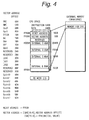
- Fig. 4 shows an example of the structure of an address space of the RISC 1.
- 64 Kbytes can be used for each of instructions and data.
- a 96-word external register can be used to exchange data between the RISC 1 and the external coprocessors.
- the control branches to FF60H and executes an instruction stored therein.
- Vector addresses are allocated every two words (four bytes). At the first word, a branch (jump) instruction is set. At the second word that is a delay slot, a "nop (no operation)" instruction or another instruction is set.
- the base address of the vector address is the value stored in the register IBR (high order eight bits).
- the vector address can be set at any location of 256 bytes.
- An offset value to be branched is set at the vector address.
- the address to be branched is obtained.
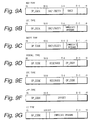
- Figs. 5A to 5G show examples of formats of instructions used in the one-chip microcomputer shown in Fig. 1.
- Fig. 5A shows the format of an MOV instruction.
- the length of the instruction is 16 bits fixed.
- This format is of two-operand type composed of an operation code (OP_CODE) and two operands (SRC1/DEST1, SRC2) . Since the instruction length is 16 bits fixed, the code efficiency can be improved.
- Fig. 5B shows the format of a LSI type (immediate instruction).
- Fig. 5C shows the format of a SHIFT type (shift instruction).
- Fig. 5D shows the format of a SYSCALL type (branch instruction).
- Fig. 5E shows the format of a CFC type (coprocessor transfer instruction).
- Fig. 5F shows the format of a JMP type (branch instruction).
- Fig. 5G shows the format of an LI type (immediate instruction).
- bit process instruction for example, a bit inverting process can be easily performed.
- the process can be effectively performed.
- the code efficiency can be further improved.
- Fig. 6 shows operations of a five-staged pipeline, an instruction bus 8, a data bus 9, and a coprocessor bus 7 (transfer means).
- the instruction bus 8, the data bus 9, and the coprocessor bus 7 are independently structured.
- data input/output of these buses is independently performed.
- Each bus is connected by an external cache (buffer) and a register of the coprocessor 2.
- the coprocessor bus 7 can be separated from the data bus so as to remove the restrictions of the extended coprocessors. Since the coprocessor bus 7 is separated from the data bus 9, as shown in Fig. 6, a load process or a store process of the coprocessor 2 can be performed independently from a conventional load process or a store process of the RISC 1. Thus, the coprocessor 2 can be released from a critical path. Consequently, the coprocessor 2 can freely use the bus (coprocessor bus 7).
- the instruction decoder/pipeline controlling portion 16 determines whether an instruction latched on the instruction bus 8 is issued to the RISC 1 or the coprocessor 2 when the signal level of the clock signal supplied from the reset/clock controlling portion 19 becomes low.
- the RISC 1 executes the instruction.
- the operation corresponding to the instruction is performed by the hardware of the coprocessor 2. At this point, the RISC 1 does not perform any process.
- Fig. 7 shows timings of which individual buses can be used after an instruction is decoded.
- the coprocessor 2 can freely use the coprocessor bus 7.
- the coprocessor 2 the first coprocessor (COP0) and the second coprocessor (COP1) can be extensionally used.
- a RISC instruction data can be transferred between the coprocessors and the general purpose registers and between the coprocessors and the memory.
- a jump instruction table is preferably used instead of a so-called interrupt vector table.
- vector addresses are set every four bytes.
- a 96-byte movable instruction table is formed.
- 24 exceptions can be defined.
- One exception is defined with four bytes.
- two bytes (one word) of the four bytes a jump instruction is set.
- the remaining two bytes (one word) are used as a delay slot. In the delay slot, a no-operation instruction or another instruction is set.
- external interrupts can be defined as follows.
- the eight external interrupts can be allocated the "round robin" mode or the "fixed" mode.
- the interrupts are cyclically processed in the order of interrupt numbers 0, 1, 2, ... , 7, 0, ... and so forth at predetermined intervals.
- the interrupts are cyclically processed in the order of the interrupt numbers 1, 2, 3, ... , 7, 0, 1, ... and so forth at the predetermined intervals.
- the eight external interrupts can be categorized as two groups of "high” and "low". In each of the "high” group and the "low” group, the eight interrupts can be allocated priority. At this point, in the "high” group or the “low” group, the "round robin" mode or the "fixed” mode can be independently allocated.
- the interrupts are cyclically processed in the order of the interrupt numbers 4, 5, 6, 7, 4, 5, ... and so forth at the predetermined intervals.
- the interrupts are cyclically processed in the order of the interrupt numbers 5, 6, 7, 4, 5, 6, ... and so forth at the predetermined intervals.
- the interrupts are cyclically processed in the order of the interrupt numbers 0, 1, 2, 3, 0, ... and so forth at the predetermined intervals.
- the interrupts are cyclically processed in the order of the interrupt numbers 1, 2, 3, 0, 1, ... and so forth at the predetermined intervals.
- interrupts can be managed in multiple levels.
- the PC Program Counter
- the interrupt process can be performed at high speed.
- a support circuit for a RETI (Return Interrupt) instruction and three-leveled interrupts is provided.
- a three-leveled interrupt stack is provided. For example, regions of several bits are formed in the register G3 (ICR) of the COP0 shown in Fig. 3. With these regions, the three-leveled interrupt stack is formed. Whenever an interrupt is executed, the values of these regions are shifted.
- a conventional conditional branch instruction is executed as one instruction.
- a conditional branch instruction is executed.
- the execution time of the comparison instruction and the conditional branch instruction is remarkably long. This is because the conditional branch is performed with a defined value in the flag register corresponding to the compared result of the comparison instruction.
- the 16-bit fixed length RISC 1 is composed of a five-staged pipeline.
- a pipeline delay takes place.
- a flag corresponding to the result of the comparison instruction is generated by the bypass circuit 12 so that the result of the comparison instruction can be immediately used for the branch instruction.
- the conditional branch operation can be performed at high speed.
- Fig. 8 shows the structure of a five-staged pipeline.
- the five-staged pipeline is composed of an IF (instruction fetch) stage, an RF (register fetch) stage, an ALU (arithmetic operation) stage, an MEM (memory transfer) stage, and a WB (register write back) stage.
- the conditional branch instruction is executed, the latest updated flag of the pipeline of which the value in the flag register is not defined is used.
- the flag is supplied from the above-described bypass circuit.
- the ALU it is determined whether or not the latest flag is valid.
- the latest flag is valid
- the result is read.
- the MEM is executed, if the latest flag is valid, data that has been loaded or stored is used. In such a manner, in each stage of the pipeline, it is determined whether the flag is valid.
- Figs. 9A to 9G show examples of formats of microcodes as an application of the formats of 16-bit fixed length instructions.
- microcodes are copyright protected, whereas binary codes of CPU instructions are not copyright protected.
- instruction scheme thereof is formats of microcodes.
- the bits 15 to 0 of the 16-bit fixed instructions are instruction scheme of the RISC.
- the hardware connected to the CPU (RISC) 1 can be controlled for multiple purposes.
- the instructions of the RISC can be used as microcodes with a bit length of 17 bits to 20 bits.
- a PLA Programmable Logic Array
- microcodes are used.
- the formats of the microcodes allow the data bus to effectively work.
- the instruction scheme of the RISC is composed of fixed length instructions, it can be treated as formats of microcodes.
- the data bus can be directly controlled.
- an instruction is analyzed.
- the top address of a microcode is calculated.
- the calculated address is supplied to a predetermined microcode and then executed.
- several bits added to the RISC instruction set are for example an instruction end bit. In such a manner, the data bus is controlled.
- Fig. 11 shows an example of the structure of a one-chip microcomputer for use with a GPS (Global Positioning System).
- the one-chip microcomputer has the above-described RISC type microprocessor, a satellite receiving LSI, a RAM, and a ROM that are integrated in one chip.
- a boot ROM/target ROM debugger 33 of the one-chip microcomputer (GPS_LSI) 31 is composed of a boot ROM and a target ROM debugger.
- the boot ROM stores a boot program that is executed when the power of the one-chip microcomputer is turned on.
- the target ROM debugger stores a debugger program that is used to perform a debugging operation.
- a data RAM 34 stores various types of data necessary for executing various processes.
- a dual port RAM 35 stores data received from a host computer (not shown) through a bus 39. In addition, the dual port RAM 35 stores data to be sent to the host computer.
- An instruction RAM/ROM 36 stores particular application programs, control programs, and so forth. By connecting a PC (Personal Computer) 38 to an SIO (Serial Input/Output) 37, programs stored in the instruction RAM/ROM 36 can be debugged.
- PC Personal Computer
- SIO Serial Input/Output
- Fig. 12 shows an example of the structure of a GPS receiving system as an application of the information processing apparatus according to the present invention.
- An antenna 41 receives a radio wave from a GPS satellite (not shown) and supplies a signal of the radio wave to a band pass filter 42.
- the band pass filter 42 passes only a predetermined frequency of the input signal.
- An amplifier 43 amplifies the output signal of the band pass filter 42 and supplies the resultant signal to a multiplying device 46.
- the multiplying device 44 multiplies the output signal of the amplifier 43 by a C/A code supplied from a C/A (Clear and Acquisition) code generator 55 and supplies the resultant signal to a band pass filter 45.
- the band pass filter 45 passes only a predetermined frequency of the output signal of the multiplying device 44.
- a multiplying device 46 multiplies the output signal of the band pass filter 45 by the output signal of a frequency multiplying device 53 (that will be described later) and supplies the resultant signal to a band pass filter 47.
- the band pass filter 47 passes only a predetermined frequency of the output signal of the multiplying device 46.
- a multiplying device 48 multiplies the output signal of the band pass filter 47 by the output signal of a frequency multiplying device 54 (that will be described later).
- a band pass filter 49 passes only a predetermined frequency of the output signal of the multiplying device 48.
- a synchronous tracking circuit 50 is composed of a PLL or the like.
- the synchronous tracking circuit 50 detects synchronization and outputs a synchronous detection signal and a reproduced carrier wave.
- a noise detection filter 51 detects and removes noise contained in the input signal.
- a synchronous acquiring circuit 52 generates a clock signal corresponding to the synchronous detection signal and the reproduced carrier wave and supplies the clock to the C/A code generator 55.
- the frequency multiplying devices 53 and 54 extract higher harmonics of the input signals, amplify the extracted higher harmonics, and supply the resultant signals to the multiplying devices 46 and 48, respectively.
- the C/A code generator 55 generates a C/A code (namely, PN (Pseudo-Noise) code) in synchronization with the clock signal supplied from the synchronous acquiring circuit 52.
- the GPS radio wave transmitted from the GPS satellite is received by the antenna 41.
- the GPS radio wave is converted into a predetermined signal.
- the resultant signal is amplified by the amplifier 43 and then supplied to the multiplying device 44.
- the GPS satellite multiplies the carrier wave by the C/A code so as to spread spectrum.
- the receiving side should multiply the received signal by the same C/A code as that of the GPS satellite so as to obtain a narrow band signal.
- the multiplying device 44 multiplies the output signal of the amplifier 43 by the C/A code generated by the C/A code generator 55 and supplies the resultant signal to the band pass filter 45.
- the band pass filter 45 passes only a predetermined frequency of the output signal of the multiplying device 44.
- the resultant signal is supplied to the multiplying device 46.
- the multiplying device 46 multiplies the output signal of the band pass filter 45 by the output signal of the frequency multiplying device 53 and supplies the resultant signal to the band pass filter 47.
- the band pass filter 47 passes only a predetermined frequency of the output signal of the multiplying device 46 and supplies the resultant signal to the multiplying device 48.
- the multiplying device 48 multiplies the output signal of the band pass filter 47 by the output signal of the frequency multiplying device 54 and supplies the resultant signal to the band pass filter 49.
- the band pass filter 49 passes only a predetermined frequency of the output signal of the multiplying device 48 and supplies the resultant signal to the synchronous tracking circuit 50.
- the output signal of the synchronous tracking circuit 50 is supplied to the noise detection filter 50.
- the noise detection filter 50 removes noise contained in the output signal of the synchronous tracking circuit 50.
- the resultant signal is supplied to the synchronous tracking circuit 50 once again.
- the synchronous tracking circuit 50 tracks the synchronization of the output signal of the input signal and outputs the synchronous detection signal and the reproduced carrier wave.
- the synchronous detection signal and the reproduced carrier wave that are output from the synchronous tracking circuit 50 are supplied to the synchronous acquiring circuit 52.
- the synchronous acquiring circuit 52 generates a clock signal with a predetermined frequency corresponding to the synchronous detection signal and the reproduced carrier wave supplied from the synchronous tracking circuit 50 and supplies the clock signal to the C/A code generator 55.
- the C/A code generator 55 generates the C/A code in synchronization with the clock signal and supplies the C/A code to the multiplying device 44. At this point, the phase of the C/A code supplied from the C/A code generator 55 is slightly shifted so that the phase of the C/A code accords with the phase of the received signal.
- the received signal is converted into a base band signal and demodulated data is obtained.
- the demodulated data is supplied from the synchronous tracking circuit 50 to the CPU (not shown).
- the above-described GPS receiving system can be structured with one chip.
- the chip can be used as the satellite receiving LSI 32 shown in Fig. 11.
- the signal received from the GPS satellite to the satellite receiving LSI 32 is supplied to the RISC 1.
- the RISC 1 executes predetermined arithmetic operations corresponding to the signal supplied from the satellite receiving LSI 32 at high speed and measures the present location of the GPS receiving system. Thereafter, the RISC 1 reads map information corresponding to the present location from a CD-ROM or the like, converts the map information into picture data, and displays a map corresponding to the picture data on a CRT (not shown).
- the RISC 1 can perform two-dimensional or three-dimensional code conversion for the picture data corresponding to the traveling direction of the GPS receiving system or a user's operation.
- the RISC 1 can synthesize a particular sound signal and output it at a proper timing.
- a navigation system can be accomplished with one chip.
- the cost of the system can be reduced.
- the power consumption of the system can be suppressed.
- the number of stages of the pipeline is five.
- the number of stages of the pipeline is not limited to five.
- the instruction length is 16 bits fixed. However, another fixed bit length may be used.
- the number of bits newly added is four. However, any number of bits may be added.
- the present invention is not limited to the GPS receiving system. Instead, the present invention can be applied for a game machine, a portable information communication unit, a multimedia unit such as a KARAOKE unit, and other types of units.
- a predetermined fixed-length instruction is decoded by a decoding means.
- the decoding process for an instruction can be performed at high speed. Consequently, the arithmetic operations can be performed at high speed.
- a first mode for cyclically executing processes corresponding to a plurality of interrupts at predetermined intervals or a second mode for successively executing the processes corresponding to the interrupts is allocated by a mode allocating means.
- the interrupt process is controlled by an interrupt controlling means corresponding to the mode allocated by the mode allocating means.
- the interrupt process can be effectively executed. Consequently, the RISC type microprocessor can be used for a controller.
- a transferring means is provided independently from a data bus of the RISC type microprocessor.
- the transferring means is dedicatedly used by the coprocessor and adapted for transferring data.
- the coprocessor can transfer data independently from the RISC type microprocessor. Consequently, the coprocessor can be released from the critical path.
- a receiving unit that receives the radio wave from a GPS satellite and a RISC type microprocessor that processes the signal corresponding to the radio wave are integrated in one chip.
Abstract
Description
- The present invention relates to a RISC type microprocessor and to an information processing apparatus including such a microprocessor. An illustrative embodiment of the invention relates to a RISC type microprocessor of which RISC technologies are applied for a conventional one-chip microcomputer so as to execute an interrupt process and a numeric operation at high speed.
- Conventional RISCs (Reduced Instruction Set Computers) have been developed as engines for computers mainly to increase the speed of arithmetic operations. The instruction length of the RISCs is normally 32 bits, fixed.
- In a one-chip microcomputer integrated with a RISC, since the code efficiency is low, the interrupt process is performed by another chip. Thus, the speed of the interrupt process is low. On the other hand, with a conventional one-chip microcomputer, arithmetic operations cannot be performed at high speed.
- In accordance with an aspect of the invention, RISC technologies are employed for a one-chip microcomputer so as to perform both the interrupt process and the arithmetic operations at high speed.
- According to one aspect of the invention, a RISC type microprocessor comprises a decoding means for decoding a predetermined fixed-length instruction. A predetermined fixed-length instruction is decoded by a decoding means. Thus, the decoding process for an instruction can be performed at high speed.
- According to another aspect of the invention, a RISC type microprocessor comprises a mode allocating means for allocating a first mode for cyclically executing processes corresponding to a plurality of interrupts at predetermined intervals or a second mode for successively executing the processes corresponding to the interrupts, and an interrupt controlling means for controlling the interrupts corresponding to the mode allocated by the mode allocating means.
- In the said other aspect a first mode for cyclically executing processes corresponding to a plurality of interrupts at predetermined intervals or a second mode for successively executing the processes corresponding to the interrupts is allocated by a mode allocating means. The interrupt process is controlled by an interrupt controlling means corresponding to the mode allocated by the mode allocating means. Thus, the interrupt process can be effectively executed.
- A further aspect of the invention provides a RISC type microprocessor comprising a transferring means provided independently from a data bus of the RISC type microprocessor, dedicatedly used by the coprocessor, and adapted for transferring data.
- In the further aspect of the invention, a transferring means is provided independently from a data bus of the RISC type microprocessor. The transferring means is dedicatedly used by the coprocessor and adapted for transferring data. Thus, the coprocessor can transfer data independently from the RISC type microprocessor.
- A yet further aspect of the invention provides an apparatus having a receiving unit for receiving a radio wave from a GPS satellite and a RISC type microprocessor for processing a signal corresponding to the radio wave received by the receiving unit, wherein the receiving unit for receiving the radio wave from for example a GPS satellite and the RISC type microprocessor for processing the signal corresponding to the radio wave are integrated in one chip.
- In the yet further aspect, a receiving unit that receives the radio wave from a GPS satellite and a RISC type microprocessor that processes the signal corresponding to the radio wave are integrated in one chip. Thus, the size of the apparatus can be reduced.
- A better understanding of the present invention will become readily apparent from the following illustrative description of the accompanying drawings, in which:
- Fig. 1 is a block diagram showing a structure of a one-chip microcomputer as an application of a RISC type microprocessor according to an embodiment of the present invention;
- Fig. 2 is a schematic diagram showing an internal structure of the
RISC 1 shown in Fig. 1; - Fig. 3 is a schematic diagram showing a structure of registers of the one-chip microcomputer shown in Fig. 1;
- Fig. 4 is a schematic diagram showing an address space of the
RISC 1; - Figs. 5A to 5G are schematic diagrams showing formats of instructions used in the
RISC 1; - Fig. 6 is a schematic diagram showing a pipeline operation of an instruction decoder/
pipeline controlling portion 16; - Fig. 7 is a schematic diagram showing an operation of a
coprocessor bus 7; - Fig. 8 is a schematic diagram showing a structure of a pipeline;
- Figs. 9A to 9G are schematic diagrams showing formats of microcodes;
- Fig. 10 is a schematic diagram for explaining the difference of the controlling method of the data bus between a CISC instruction set and a RISC instruction set;
- Fig. 11 is a block diagram showing an example of the structure of a GPS-LSI; and
- Fig. 12 is a block diagram showing an example of the structure of a GPS receiving system.
- Fig. 1 shows a structure of a one-chip microcomputer as an application of a RISC type microprocessor according to an embodiment of the present invention. A RISC (Reduced Instruction Set Computer) 1 that composes the one-chip microcomputer can input eight external interrupts, a nonmaskable interrupt nmi, and a power management interrupt pmi. In addition, the
RISC 1 can input a reset signal and a clock signal from the outside. - When the reset signal is input to the
RISC 1, it executes a program stored in an IPL (Initial Program Loader)-ROM 3. When this program is executed, amemory controller 5 gets started through a register of a coprocessor (co_pro) 2. Thus, an operating system is loaded from an auxiliary storing unit (not shown) to acode buffer 4, adata buffer 5, and a main memory (not shown). - Fig. 2 shows an example of the structure of the
RISC 1 shown in Fig. 1. In theRISC - An ALU (Arithmetic and Logic Unit) is composed of a barrel shifter or the like. The ALU performs a predetermined logic operation and an arithmetic operation. A high speed multiplying device/high speed dividing device 14 executes a multiplying process for multiplying 16-bit data by 16-bit data in one cycle, a dividing process for dividing 32-bit data by 16-bit data in 13 cycles, and a dividing process for dividing 16-bit data by 16-bit data in eight cycles.
- An
address calculating portion 15 calculates an address with a program counter or the like. An instruction decoder/pipeline controlling portion 16 (decoding means) interprets for example a 16-bit fixed length instruction read from the memory and performs a pipeline process with a five-staged pipeline. - 11 16-bit dedicated control registers 17 (mode allocating means) are provided. The dedicated control registers 17 store status information (flag information), interrupt control information, and so forth. An
interrupt controller 18 controls an interrupt process corresponding to the interrupt control information stored in thededicated control register 17. A reset/clock controlling portion 19 generates a reset signal and a clock signal and supplies these signals to each portion of theRISC 1. - Fig. 3 shows a register map of the one-chip microcomputer shown in Fig. 1. In this case, two coprocessors (COP0 and COP1) are extensionally used. The RISC (CPU) 1 has 32 general purpose registers. 32 control registers of the first coprocessor (COP0) 2 are used (mapped) as internal control registers for the CPU. Thus, the user can use only the remaining 32 control registers. In addition, the user can use 64 control registers of the second coprocessor (COP1) (not shown) without any restriction.
- The general purpose registers can be used as registers for arithmetic operations other than special instructions. A register ACC (R1) can be used for an immediate operand and an operand in a bit process. As an exception, a register SP (R30) can be used as a stack pointer for a "RET" instruction. A register ISP (R31) can be used as a stack pointer for an interrupt process, an exception process, and a "RETI" instruction. The initial values of these general purpose registers (including the register ACC, the register SP, and the register ISP) are undefined.
- As shown in Fig. 3, a total of 128 registers of registers G31 to G0 and C31 to C0 of the first coprocessor (COP0) 2 and registers G31 to G0 and C31 to C0 of the second coprocessor (COP1) can be extensionally used. Data transfer among the registers of the coprocessors, the general purpose registers, and the memory is defined by instructions.
- A total of 96 registers of the registers C31 to C0 of the first coprocessor and the registers G31 to G0 and C31 to C0 of the second coprocessor can be used as external extension registers. 11 of the registers G31 to G0 of the first coprocessor function as control registers for the CPU. The remaining 21 registers are reserved for further extensions.
- An SR (Status Register) stores a flag corresponding to the result of an arithmetic operation or the like. An MCR (Machine Control Register) is used for a machine control. For example, data that allocates 32-bit divisions is stored in the MCR. An IBR (Interrupt Base Register) stores the base address of an interrupt vector table. A JBR (Jump Base Register) is used when a special jump instruction is executed and a branch is performed. An ICR (Interrupt Control Register) is used for an interrupt control. The ICR structures a three-level interrupt stack.
- An IMR0 (Interrupt Mode Register 0) is used for an external interrupt mode control. For example, a "round robin" mode or "fixed" mode (that will be described later) is set to the IMR0. An IMR1 (Interrupt Mode Register 1) is used for categorizing eight external interrupts as groups. A DAB0 (Data Address Break 0) is used for storing a break address of a data buffer. An IAB1 (Instruction Address Break 1) is used for storing a break address of an instruction buffer. An IAB2 (Instruction Address Break 2), is used for storing a break address of an instruction buffer. An XDDD (Extended Divide Divident) is used for storing
high order 16 bits of a 32-bit divident when an extended division instruction is executed. - Each of the first coprocessor and the second coprocessor has around 30 operation codes that the user can extensionally use. These operation codes can be easily executed by a "DW" instruction of the assembler. The CPU supports an exception process of which the coprocessors are not used. The hardware of the coprocessors can be simulated by software.
- Fig. 4 shows an example of the structure of an address space of the
RISC 1. 64 Kbytes can be used for each of instructions and data. To exchange data between theRISC 1 and the external coprocessors, a 96-word external register can be used. When theRISC 1 receives an external reset, the control branches to FF60H and executes an instruction stored therein. Vector addresses are allocated every two words (four bytes). At the first word, a branch (jump) instruction is set. At the second word that is a delay slot, a "nop (no operation)" instruction or another instruction is set. - The base address of the vector address is the value stored in the register IBR (high order eight bits). The vector address can be set at any location of 256 bytes. An offset value to be branched is set at the vector address. Corresponding to the offset value and the base address stored in the register IBR (for example, by ORing them), the address to be branched is obtained.
- Figs. 5A to 5G show examples of formats of instructions used in the one-chip microcomputer shown in Fig. 1. Fig. 5A shows the format of an MOV instruction. The length of the instruction is 16 bits fixed. This format is of two-operand type composed of an operation code (OP_CODE) and two operands (SRC1/DEST1, SRC2) . Since the instruction length is 16 bits fixed, the code efficiency can be improved.
- Fig. 5B shows the format of a LSI type (immediate instruction). Fig. 5C shows the format of a SHIFT type (shift instruction). Fig. 5D shows the format of a SYSCALL type (branch instruction). Fig. 5E shows the format of a CFC type (coprocessor transfer instruction). Fig. 5F shows the format of a JMP type (branch instruction). Fig. 5G shows the format of an LI type (immediate instruction).
- In addition, a bit process instruction is provided. With the bit process instruction, for example, a bit inverting process can be easily performed. Thus, when the one-chip microcomputer is used as a controller, the process can be effectively performed. Moreover, with the above-described immediate instruction, the code efficiency can be further improved.
- Fig. 6 shows operations of a five-staged pipeline, an
instruction bus 8, adata bus 9, and a coprocessor bus 7 (transfer means). As shown in Fig. 1, theinstruction bus 8, thedata bus 9, and thecoprocessor bus 7 are independently structured. In addition, data input/output of these buses is independently performed. Each bus is connected by an external cache (buffer) and a register of thecoprocessor 2. - When the bus width is 16 bits, even if such buses are independently structured, the total bus width is not large. Thus, as described above, the
coprocessor bus 7 can be separated from the data bus so as to remove the restrictions of the extended coprocessors. Since thecoprocessor bus 7 is separated from thedata bus 9, as shown in Fig. 6, a load process or a store process of thecoprocessor 2 can be performed independently from a conventional load process or a store process of theRISC 1. Thus, thecoprocessor 2 can be released from a critical path. Consequently, thecoprocessor 2 can freely use the bus (coprocessor bus 7). - The instruction decoder/
pipeline controlling portion 16 determines whether an instruction latched on theinstruction bus 8 is issued to theRISC 1 or thecoprocessor 2 when the signal level of the clock signal supplied from the reset/clock controlling portion 19 becomes low. When the instruction is issued to theRISC 1, theRISC 1 executes the instruction. When the instruction is issued to thecoprocessor 2, the operation corresponding to the instruction is performed by the hardware of thecoprocessor 2. At this point, theRISC 1 does not perform any process. - Fig. 7 shows timings of which individual buses can be used after an instruction is decoded. Thus, the
coprocessor 2 can freely use thecoprocessor bus 7. - In addition, as the
coprocessor 2, the first coprocessor (COP0) and the second coprocessor (COP1) can be extensionally used. With a RISC instruction, data can be transferred between the coprocessors and the general purpose registers and between the coprocessors and the memory. - In the 16-bit fixed length RISC processor, to effectively process an interrupt without stopping the five-staged pipeline, a jump instruction table is preferably used instead of a so-called interrupt vector table. In the address space shown in Fig. 4, as described above, vector addresses are set every four bytes. A 96-byte movable instruction table is formed. In the table, 24 exceptions can be defined. One exception is defined with four bytes. In two bytes (one word) of the four bytes, a jump instruction is set. The remaining two bytes (one word) are used as a delay slot. In the delay slot, a no-operation instruction or another instruction is set.
- As shown in Fig. 4, only three instruction exceptions, seven internal exceptions, two non-maskable interrupts, and eight external interrupts are defined. These exceptions and interrupts can be effectively controlled.
- In addition, external interrupts can be defined as follows. In other words, the eight external interrupts can be allocated the "round robin" mode or the "fixed" mode. In the "round robin" mode, when the initial value is set to 0, the interrupts are cyclically processed in the order of interrupt
numbers numbers - In the "fixed" mode, when the initial value is set to 0, the interrupts are successively processed in the order of the interrupt
numbers numbers - Alternatively, the eight external interrupts can be categorized as two groups of "high" and "low". In each of the "high" group and the "low" group, the eight interrupts can be allocated priority. At this point, in the "high" group or the "low" group, the "round robin" mode or the "fixed" mode can be independently allocated.
- In the case that the "round robin" mode is allocated to the four external interrupts in the "high" group, when the initial value is set to 4, the interrupts are cyclically processed in the order of the interrupt
numbers numbers - In the case that the "fixed" mode is allocated to the four external interrupts in the "high" group, when the initial value is set to 4, the interrupts are successively processed in the order of the interrupt
numbers numbers - In the case that the "round robin" mode is allocated to the four external interrupts in the "low" group, when the initial value. is set to 0, the interrupts are cyclically processed in the order of the interrupt
numbers numbers - In the case that the "fixed" mode is allocated to the four external interrupts in the "low" group, when the initial value is set to 0, the interrupts are successively processed in the order of the interrupt
numbers numbers - When an interrupt process is executed with the register R31 as the ISP (Interrupt Stack Pointer) as shown in Fig. 3, interrupts can be managed in multiple levels. In other words, when an interrupt takes place, the PC (Program Counter) is saved to a stack so as to prohibit an external interrupt. Thus, the interrupt process can be performed at high speed. In addition, a support circuit for a RETI (Return Interrupt) instruction and three-leveled interrupts is provided. In other words, a three-leveled interrupt stack is provided. For example, regions of several bits are formed in the register G3 (ICR) of the COP0 shown in Fig. 3. With these regions, the three-leveled interrupt stack is formed. Whenever an interrupt is executed, the values of these regions are shifted.
- In a 32-bit fixed length RISC, a conventional conditional branch instruction is executed as one instruction. In a classic CISC, after a comparison instruction is executed, a conditional branch instruction is executed. Thus, the execution time of the comparison instruction and the conditional branch instruction is remarkably long. This is because the conditional branch is performed with a defined value in the flag register corresponding to the compared result of the comparison instruction.
- On the other hand, in a 16-bit fixed length RISC, since the instruction length is short, a conditional branch instruction cannot be executed as one instruction. Thus, after the comparison instruction is executed, the branch instruction is executed.
- The 16-bit
fixed length RISC 1 is composed of a five-staged pipeline. When a defined value in the flag register is used, after the comparison instruction is executed, until the conditional branch instruction is executed, a pipeline delay takes place. To prevent the pipeline delay, a flag corresponding to the result of the comparison instruction is generated by the bypass circuit 12 so that the result of the comparison instruction can be immediately used for the branch instruction. Thus, the conditional branch operation can be performed at high speed. - Fig. 8 shows the structure of a five-staged pipeline. As shown in Fig. 8, the five-staged pipeline is composed of an IF (instruction fetch) stage, an RF (register fetch) stage, an ALU (arithmetic operation) stage, an MEM (memory transfer) stage, and a WB (register write back) stage. When the conditional branch instruction is executed, the latest updated flag of the pipeline of which the value in the flag register is not defined is used. The flag is supplied from the above-described bypass circuit. When the ALU is executed, it is determined whether or not the latest flag is valid. When the latest flag is valid, the result is read. When the MEM is executed, if the latest flag is valid, data that has been loaded or stored is used. In such a manner, in each stage of the pipeline, it is determined whether the flag is valid.
- Figs. 9A to 9G show examples of formats of microcodes as an application of the formats of 16-bit fixed length instructions. Generally, microcodes are copyright protected, whereas binary codes of CPU instructions are not copyright protected. However, in the case of the RISC, since instruction scheme thereof is formats of microcodes. Thus, when several bits (for example, four bits) are added to an instruction of the RISC and used for multiple purposes, complete formats of microcodes are obtained. The
bits 15 to 0 of the 16-bit fixed instructions are instruction scheme of the RISC. - By adding several bits (bit -1 to -4) to a 16-bit fixed length instruction, the hardware connected to the CPU (RISC) 1 can be controlled for multiple purposes. Thus, the instructions of the RISC can be used as microcodes with a bit length of 17 bits to 20 bits.
- To accomplish a complicated RISC instruction set, a PLA (Programmable Logic Array) or the like may be used. However, normally, microcodes are used. The formats of the microcodes allow the data bus to effectively work. On the other hand, the instruction scheme of the RISC is composed of fixed length instructions, it can be treated as formats of microcodes. By slightly modifying the instruction scheme of the RISC, a complicated CISC instruction set can be accomplished. In other words, the instruction scheme of the RISC allows the data bus to effectively work.
- Thus, as shown in Fig. 10, with the RISC instruction set, the data bus can be directly controlled. On the other hand, in the case of the CISC instruction set, an instruction is analyzed. Next, the top address of a microcode is calculated. The calculated address is supplied to a predetermined microcode and then executed. In the microcode format, several bits added to the RISC instruction set are for example an instruction end bit. In such a manner, the data bus is controlled.
- Fig. 11 shows an example of the structure of a one-chip microcomputer for use with a GPS (Global Positioning System). The one-chip microcomputer has the above-described RISC type microprocessor, a satellite receiving LSI, a RAM, and a ROM that are integrated in one chip. A boot ROM/
target ROM debugger 33 of the one-chip microcomputer (GPS_LSI) 31 is composed of a boot ROM and a target ROM debugger. The boot ROM stores a boot program that is executed when the power of the one-chip microcomputer is turned on. The target ROM debugger stores a debugger program that is used to perform a debugging operation. - A
data RAM 34 stores various types of data necessary for executing various processes. Adual port RAM 35 stores data received from a host computer (not shown) through abus 39. In addition, thedual port RAM 35 stores data to be sent to the host computer. An instruction RAM/ROM 36 stores particular application programs, control programs, and so forth. By connecting a PC (Personal Computer) 38 to an SIO (Serial Input/Output) 37, programs stored in the instruction RAM/ROM 36 can be debugged. - Fig. 12 shows an example of the structure of a GPS receiving system as an application of the information processing apparatus according to the present invention. An
antenna 41 receives a radio wave from a GPS satellite (not shown) and supplies a signal of the radio wave to aband pass filter 42. Theband pass filter 42 passes only a predetermined frequency of the input signal. Anamplifier 43 amplifies the output signal of theband pass filter 42 and supplies the resultant signal to a multiplyingdevice 46. - The multiplying
device 44 multiplies the output signal of theamplifier 43 by a C/A code supplied from a C/A (Clear and Acquisition)code generator 55 and supplies the resultant signal to aband pass filter 45. Theband pass filter 45 passes only a predetermined frequency of the output signal of the multiplyingdevice 44. A multiplyingdevice 46 multiplies the output signal of theband pass filter 45 by the output signal of a frequency multiplying device 53 (that will be described later) and supplies the resultant signal to aband pass filter 47. Theband pass filter 47 passes only a predetermined frequency of the output signal of the multiplyingdevice 46. A multiplyingdevice 48 multiplies the output signal of theband pass filter 47 by the output signal of a frequency multiplying device 54 (that will be described later). Aband pass filter 49 passes only a predetermined frequency of the output signal of the multiplyingdevice 48. - A
synchronous tracking circuit 50 is composed of a PLL or the like. Thesynchronous tracking circuit 50 detects synchronization and outputs a synchronous detection signal and a reproduced carrier wave. Anoise detection filter 51 detects and removes noise contained in the input signal. A synchronous acquiringcircuit 52 generates a clock signal corresponding to the synchronous detection signal and the reproduced carrier wave and supplies the clock to the C/Acode generator 55. Thefrequency multiplying devices devices code generator 55 generates a C/A code (namely, PN (Pseudo-Noise) code) in synchronization with the clock signal supplied from the synchronous acquiringcircuit 52. - Next, the operation of the GPS receiving system will be described. The GPS radio wave transmitted from the GPS satellite is received by the
antenna 41. The GPS radio wave is converted into a predetermined signal. The resultant signal is amplified by theamplifier 43 and then supplied to the multiplyingdevice 44. The GPS satellite multiplies the carrier wave by the C/A code so as to spread spectrum. Thus, the receiving side should multiply the received signal by the same C/A code as that of the GPS satellite so as to obtain a narrow band signal. In other words, the multiplyingdevice 44 multiplies the output signal of theamplifier 43 by the C/A code generated by the C/Acode generator 55 and supplies the resultant signal to theband pass filter 45. - The
band pass filter 45 passes only a predetermined frequency of the output signal of the multiplyingdevice 44. The resultant signal is supplied to the multiplyingdevice 46. The multiplyingdevice 46 multiplies the output signal of theband pass filter 45 by the output signal of thefrequency multiplying device 53 and supplies the resultant signal to theband pass filter 47. Theband pass filter 47 passes only a predetermined frequency of the output signal of the multiplyingdevice 46 and supplies the resultant signal to the multiplyingdevice 48. - The multiplying
device 48 multiplies the output signal of theband pass filter 47 by the output signal of thefrequency multiplying device 54 and supplies the resultant signal to theband pass filter 49. Theband pass filter 49 passes only a predetermined frequency of the output signal of the multiplyingdevice 48 and supplies the resultant signal to thesynchronous tracking circuit 50. The output signal of thesynchronous tracking circuit 50 is supplied to thenoise detection filter 50. Thenoise detection filter 50 removes noise contained in the output signal of thesynchronous tracking circuit 50. The resultant signal is supplied to thesynchronous tracking circuit 50 once again. Thesynchronous tracking circuit 50 tracks the synchronization of the output signal of the input signal and outputs the synchronous detection signal and the reproduced carrier wave. - The synchronous detection signal and the reproduced carrier wave that are output from the
synchronous tracking circuit 50 are supplied to the synchronous acquiringcircuit 52. The synchronous acquiringcircuit 52 generates a clock signal with a predetermined frequency corresponding to the synchronous detection signal and the reproduced carrier wave supplied from thesynchronous tracking circuit 50 and supplies the clock signal to the C/Acode generator 55. The C/Acode generator 55 generates the C/A code in synchronization with the clock signal and supplies the C/A code to the multiplyingdevice 44. At this point, the phase of the C/A code supplied from the C/Acode generator 55 is slightly shifted so that the phase of the C/A code accords with the phase of the received signal. - In such a manner, the received signal is converted into a base band signal and demodulated data is obtained. The demodulated data is supplied from the
synchronous tracking circuit 50 to the CPU (not shown). - The above-described GPS receiving system can be structured with one chip. The chip can be used as the
satellite receiving LSI 32 shown in Fig. 11. - In this case, the signal received from the GPS satellite to the
satellite receiving LSI 32 is supplied to theRISC 1. TheRISC 1 executes predetermined arithmetic operations corresponding to the signal supplied from thesatellite receiving LSI 32 at high speed and measures the present location of the GPS receiving system. Thereafter, theRISC 1 reads map information corresponding to the present location from a CD-ROM or the like, converts the map information into picture data, and displays a map corresponding to the picture data on a CRT (not shown). In addition, theRISC 1 can perform two-dimensional or three-dimensional code conversion for the picture data corresponding to the traveling direction of the GPS receiving system or a user's operation. Moreover, when the GPS receiving system approaches an intersection, theRISC 1 can synthesize a particular sound signal and output it at a proper timing. - As described above, when the
RISC 1 and thesatellite receiving LSI 32 are integrated in one chip, a navigation system can be accomplished with one chip. In addition, with the one-chip structure, the cost of the system can be reduced. Moreover, the power consumption of the system can be suppressed. - In the above-described embodiment, the number of stages of the pipeline is five. However, the number of stages of the pipeline is not limited to five.
- In the above-described embodiment, the instruction length is 16 bits fixed. However, another fixed bit length may be used.
- In the above-described embodiment, when an instruction of the
RISC 1 is used as a microcode, the number of bits newly added is four. However, any number of bits may be added. - In the above-described embodiment, an example of the structure of the one-chip microcomputer using the RISC processor that can be used in the GPS receiving system is shown. However, the present invention is not limited to the GPS receiving system. Instead, the present invention can be applied for a game machine, a portable information communication unit, a multimedia unit such as a KARAOKE unit, and other types of units.
- In the RISC type microprocessor of one aspect of the invention a predetermined fixed-length instruction is decoded by a decoding means. Thus, the decoding process for an instruction can be performed at high speed. Consequently, the arithmetic operations can be performed at high speed.
- In the RISC type microprocessor of another aspect of the invention a first mode for cyclically executing processes corresponding to a plurality of interrupts at predetermined intervals or a second mode for successively executing the processes corresponding to the interrupts is allocated by a mode allocating means. The interrupt process is controlled by an interrupt controlling means corresponding to the mode allocated by the mode allocating means. Thus, the interrupt process can be effectively executed. Consequently, the RISC type microprocessor can be used for a controller.
- In the RISC type microprocessor of a further aspect of the invention a transferring means is provided independently from a data bus of the RISC type microprocessor. The transferring means is dedicatedly used by the coprocessor and adapted for transferring data. Thus, the coprocessor can transfer data independently from the RISC type microprocessor. Consequently, the coprocessor can be released from the critical path.
- In the RISC type microprocessor of a yet further aspect of the invention a receiving unit that receives the radio wave from a GPS satellite and a RISC type microprocessor that processes the signal corresponding to the radio wave are integrated in one chip. Thus, the size of the apparatus can be reduced. Consequently, the power consumption can be reduced.
- Having described specific preferred embodiments of the present invention with reference to the accompanying drawings, it is to be understood that the invention is not limited to those precise embodimenta, and that various changes and modifications may be effected therein by one skilled in the art without departing from the scope or the spirit of the invention as defined in the appended claims.
Claims (9)
- A RISC type microprocessor for performing a pipeline control, comprising:
decoding means for decoding a predetermined fixed-length instruction. - The RISC type microprocessor as set forth in claim 1,
wherein the length of the instruction is 16 bits. - The RISC type microprocessor as set forth in claim 1, further comprising:
information supplying means for suppling information corresponding to the execution result of a first instruction to a second instruction executed after the first instruction. - The RISC type microprocessor as set forth in claim 1,
wherein the instructions include an instruction for performing a bit process. - The RISC type microprocessor as set forth in claim 1,
wherein the instructions include an instruction for performing an immediate operation. - A RISC type microprocessor for performing a pipeline control, comprising:mode allocating means for allocating a first mode for cyclically executing processes corresponding to a plurality of interrupts at predetermined intervals or a second mode for successively executing the processes corresponding to the interrupts; andinterrupt controlling means for controlling the interrupts corresponding to the mode allocated by said mode allocating means.
- The RISC type microprocessor as set forth in claim 6,
wherein said interrupt controlling means is adapted for saving particular information to a stack upon occurrence of an interrupt and fetching the particular information from the stack upon completion of the interrupt process. - A RISC type microprocessor having a coprocessor, comprising:
transferring means provided independently from a data bus of the RISC type microprocessor, dedicatedly used by the coprocessor, and adapted for transferring data. - An information processing apparatus having a receiving unit for receiving a radio wave from a GPS satellite and a RISC type microprocessor for processing a signal corresponding to the radio wave received by the receiving unit,
wherein the receiving unit for receiving the radio wave from the GPS satellite and the RISC type microprocessor for processing the signal corresponding to the radio wave are integrated in one chip.
Applications Claiming Priority (3)
| Application Number | Priority Date | Filing Date | Title |
|---|---|---|---|
| JP22503695 | 1995-09-01 | ||
| JP225036/95 | 1995-09-01 | ||
| JP7225036A JPH0969047A (en) | 1995-09-01 | 1995-09-01 | Risc type microprocessor and information processor |
Publications (2)
| Publication Number | Publication Date |
|---|---|
| EP0762272A2 true EP0762272A2 (en) | 1997-03-12 |
| EP0762272A3 EP0762272A3 (en) | 2001-03-14 |
Family
ID=16823055
Family Applications (1)
| Application Number | Title | Priority Date | Filing Date |
|---|---|---|---|
| EP96306284A Withdrawn EP0762272A3 (en) | 1995-09-01 | 1996-08-30 | Microprocessors and apparatus including same |
Country Status (4)
| Country | Link |
|---|---|
| US (4) | US6067614A (en) |
| EP (1) | EP0762272A3 (en) |
| JP (1) | JPH0969047A (en) |
| KR (1) | KR970016953A (en) |
Cited By (3)
| Publication number | Priority date | Publication date | Assignee | Title |
|---|---|---|---|---|
| GB2461848A (en) * | 2008-07-10 | 2010-01-20 | Cambridge Consultants | Processor with a privileged stack pointer and a stack pointer used in privileged and non-privileged modes |
| US9645949B2 (en) | 2008-07-10 | 2017-05-09 | Cambridge Consultants Ltd. | Data processing apparatus using privileged and non-privileged modes with multiple stacks |
| US9652241B2 (en) | 2007-04-10 | 2017-05-16 | Cambridge Consultants Ltd. | Data processing apparatus with instruction encodings to enable near and far memory access modes |
Families Citing this family (24)
| Publication number | Priority date | Publication date | Assignee | Title |
|---|---|---|---|---|
| JPH0969047A (en) * | 1995-09-01 | 1997-03-11 | Sony Corp | Risc type microprocessor and information processor |
| WO2000043868A1 (en) * | 1999-01-20 | 2000-07-27 | Hitachi, Ltd. | Data processor and device for arithmetic operation |
| US6732203B2 (en) * | 2000-01-31 | 2004-05-04 | Intel Corporation | Selectively multiplexing memory coupling global bus data bits to narrower functional unit coupling local bus |
| KR100602374B1 (en) * | 2000-08-31 | 2006-07-14 | 어보브반도체 주식회사 | Risc processor for raising code density using stack architecture |
| GB2370149A (en) * | 2000-12-14 | 2002-06-19 | World Information On Net | Method of displaying advertisements on a vehicle |
| US20040078608A1 (en) * | 2001-04-02 | 2004-04-22 | Ruban Kanapathippillai | Method and apparatus for power reduction in a digital signal processor integrated circuit |
| US20030216846A1 (en) * | 2002-05-17 | 2003-11-20 | Ryan Chang | Car computer operation apparatus |
| US20040039940A1 (en) * | 2002-08-23 | 2004-02-26 | Koninklijke Philips Electronics N.V. | Hardware-based packet filtering accelerator |
| US6952573B2 (en) * | 2003-09-17 | 2005-10-04 | Motorola, Inc. | Wireless receiver with stacked, single chip architecture |
| US7365680B2 (en) * | 2004-02-10 | 2008-04-29 | Sirf Technology, Inc. | Location services system that reduces auto-correlation or cross-correlation in weak signals |
| US7404178B2 (en) | 2004-02-18 | 2008-07-22 | Hewlett-Packard Development Company, L.P. | ROM-embedded debugging of computer |
| US7428259B2 (en) * | 2005-05-06 | 2008-09-23 | Sirf Technology Holdings, Inc. | Efficient and flexible GPS receiver baseband architecture |
| CN1878055B (en) * | 2005-06-07 | 2010-11-03 | 北京握奇数据系统有限公司 | Separation type mass data encryption/decryption device and implementing method therefor |
| US8189774B2 (en) * | 2006-01-06 | 2012-05-29 | Fujitsu Semiconductor Limited | Processors for network communications |
| US8733718B2 (en) * | 2012-05-10 | 2014-05-27 | Peter A. CORSI | Non-invasive roof mounting adaptor and method for installing same |
| US9160468B1 (en) * | 2012-06-15 | 2015-10-13 | Maxlinear, Inc. | Method and system for reconfigurable time-interleaved ADC for direct conversion K-band and L-band I/Q |
| US10936713B2 (en) * | 2015-12-17 | 2021-03-02 | The Charles Stark Draper Laboratory, Inc. | Techniques for metadata processing |
| US10235176B2 (en) | 2015-12-17 | 2019-03-19 | The Charles Stark Draper Laboratory, Inc. | Techniques for metadata processing |
| WO2019152792A1 (en) | 2018-02-02 | 2019-08-08 | Dover Microsystems, Inc. | Systems and methods for policy linking and/or loading for secure initialization |
| WO2019152772A1 (en) | 2018-02-02 | 2019-08-08 | The Charles Stark Draper Laboratory, Inc. | Systems and methods for policy execution processing |
| WO2019213061A1 (en) | 2018-04-30 | 2019-11-07 | Dover Microsystems, Inc. | Systems and methods for checking safety properties |
| TW202022679A (en) | 2018-11-06 | 2020-06-16 | 美商多佛微系統公司 | Systems and methods for stalling host processor |
| US11680678B2 (en) | 2018-12-03 | 2023-06-20 | Peter A. CORSI | Non-invasive roof mounting adapter plate and method for installing same |
| WO2020132012A1 (en) | 2018-12-18 | 2020-06-25 | Dover Microsystems, Inc. | Systems and methods for data lifecycle protection |
Citations (8)
| Publication number | Priority date | Publication date | Assignee | Title |
|---|---|---|---|---|
| EP0042442A1 (en) * | 1979-12-29 | 1981-12-30 | Fujitsu Limited | Information processing system |
| US4342082A (en) * | 1977-01-13 | 1982-07-27 | International Business Machines Corp. | Program instruction mechanism for shortened recursive handling of interruptions |
| US4445118A (en) * | 1981-05-22 | 1984-04-24 | The United States Of America As Represented By The Administrator Of The National Aeronautics And Space Administration | Navigation system and method |
| US4615019A (en) * | 1981-11-13 | 1986-09-30 | Ing. C. Olivetti & C., S.P.A. | Data processing system with interrupt facilities |
| EP0430520A2 (en) * | 1989-11-27 | 1991-06-05 | Raytheon Company | Apparatus and method for short cycling sequences of a P-code generator |
| EP0586847A1 (en) * | 1992-08-10 | 1994-03-16 | Siemens Aktiengesellschaft | Method for interrupt control of processes in communication systems |
| EP0602886A2 (en) * | 1992-12-18 | 1994-06-22 | Xerox Corporation | Masks for selecting multi-bit components in a composite operand |
| US5442577A (en) * | 1994-03-08 | 1995-08-15 | Exponential Technology, Inc. | Sign-extension of immediate constants in an alu |
Family Cites Families (26)
| Publication number | Priority date | Publication date | Assignee | Title |
|---|---|---|---|---|
| IT998437B (en) * | 1973-08-22 | 1976-01-20 | Honeywell Inf Systems | ACCESS SYSTEM WITH VARIABLE CYCLIC SCANNING OF THE INTERRUPT REQUESTS |
| US4181941A (en) * | 1978-03-27 | 1980-01-01 | Godsey Ernest E | Interrupt system and method |
| US4811345A (en) * | 1986-12-16 | 1989-03-07 | Advanced Micro Devices, Inc. | Methods and apparatus for providing a user oriented microprocessor test interface for a complex, single chip, general purpose central processing unit |
| US4851990A (en) * | 1987-02-09 | 1989-07-25 | Advanced Micro Devices, Inc. | High performance processor interface between a single chip processor and off chip memory means having a dedicated and shared bus structure |
| US4862407A (en) * | 1987-10-05 | 1989-08-29 | Motorola, Inc. | Digital signal processing apparatus |
| US4959781A (en) * | 1988-05-16 | 1990-09-25 | Stardent Computer, Inc. | System for assigning interrupts to least busy processor that already loaded same class of interrupt routines |
| EP0365188B1 (en) | 1988-10-18 | 1996-09-18 | Hewlett-Packard Company | Central processor condition code method and apparatus |
| US4953930A (en) * | 1989-03-15 | 1990-09-04 | Ramtech, Inc. | CPU socket supporting socket-to-socket optical communications |
| US5590365A (en) | 1990-03-30 | 1996-12-31 | Kabushiki Kaisha Toshiba | Pipeline information processing circuit for floating point operations |
| US5201056A (en) * | 1990-05-02 | 1993-04-06 | Motorola, Inc. | RISC microprocessor architecture with multi-bit tag extended instructions for selectively attaching tag from either instruction or input data to arithmetic operation output |
| JPH0437927A (en) * | 1990-06-01 | 1992-02-07 | Sony Corp | Processor processing method |
| US5287523A (en) * | 1990-10-09 | 1994-02-15 | Motorola, Inc. | Method for servicing a peripheral interrupt request in a microcontroller |
| EP0503514B1 (en) * | 1991-03-11 | 1998-11-18 | Silicon Graphics, Inc. | Backward-compatible computer architecture with extended word size and address space |
| US5542076A (en) * | 1991-06-14 | 1996-07-30 | Digital Equipment Corporation | Method and apparatus for adaptive interrupt servicing in data processing system |
| US5659797A (en) * | 1991-06-24 | 1997-08-19 | U.S. Philips Corporation | Sparc RISC based computer system including a single chip processor with memory management and DMA units coupled to a DRAM interface |
| US5430850A (en) * | 1991-07-22 | 1995-07-04 | Massachusetts Institute Of Technology | Data processing system with synchronization coprocessor for multiple threads |
| US5574872A (en) * | 1991-12-10 | 1996-11-12 | Intel Corporation | Method and apparatus for controlling the saving of pipelines in pipelined processors during trap handling |
| EP0602858A1 (en) * | 1992-12-18 | 1994-06-22 | International Business Machines Corporation | Apparatus and method for servicing interrupts in a multiprocessor system |
| US5481725A (en) * | 1993-08-03 | 1996-01-02 | Intel Corporation | Method for providing programmable interrupts for embedded hardware used with programmable interrupt controllers |
| US5574927A (en) * | 1994-03-25 | 1996-11-12 | International Meta Systems, Inc. | RISC architecture computer configured for emulation of the instruction set of a target computer |
| US5530825A (en) * | 1994-04-15 | 1996-06-25 | Motorola, Inc. | Data processor with branch target address cache and method of operation |
| US5826052A (en) * | 1994-04-29 | 1998-10-20 | Advanced Micro Devices, Inc. | Method and apparatus for concurrent access to multiple physical caches |
| US5566073A (en) * | 1994-07-11 | 1996-10-15 | Margolin; Jed | Pilot aid using a synthetic environment |
| US5608886A (en) | 1994-08-31 | 1997-03-04 | Exponential Technology, Inc. | Block-based branch prediction using a target finder array storing target sub-addresses |
| JPH0895798A (en) * | 1994-09-29 | 1996-04-12 | Fujitsu Ltd | Data processor |
| JPH0969047A (en) * | 1995-09-01 | 1997-03-11 | Sony Corp | Risc type microprocessor and information processor |
-
1995
- 1995-09-01 JP JP7225036A patent/JPH0969047A/en not_active Withdrawn
-
1996
- 1996-08-30 EP EP96306284A patent/EP0762272A3/en not_active Withdrawn
- 1996-09-02 KR KR1019960037786A patent/KR970016953A/en not_active Application Discontinuation
-
1998
- 1998-02-20 US US09/026,516 patent/US6067614A/en not_active Expired - Lifetime
- 1998-02-20 US US09/027,025 patent/US6314508B1/en not_active Expired - Lifetime
- 1998-02-20 US US09/027,371 patent/US6256701B1/en not_active Expired - Lifetime
- 1998-11-25 US US09/200,101 patent/US6298432B1/en not_active Expired - Lifetime
Patent Citations (8)
| Publication number | Priority date | Publication date | Assignee | Title |
|---|---|---|---|---|
| US4342082A (en) * | 1977-01-13 | 1982-07-27 | International Business Machines Corp. | Program instruction mechanism for shortened recursive handling of interruptions |
| EP0042442A1 (en) * | 1979-12-29 | 1981-12-30 | Fujitsu Limited | Information processing system |
| US4445118A (en) * | 1981-05-22 | 1984-04-24 | The United States Of America As Represented By The Administrator Of The National Aeronautics And Space Administration | Navigation system and method |
| US4615019A (en) * | 1981-11-13 | 1986-09-30 | Ing. C. Olivetti & C., S.P.A. | Data processing system with interrupt facilities |
| EP0430520A2 (en) * | 1989-11-27 | 1991-06-05 | Raytheon Company | Apparatus and method for short cycling sequences of a P-code generator |
| EP0586847A1 (en) * | 1992-08-10 | 1994-03-16 | Siemens Aktiengesellschaft | Method for interrupt control of processes in communication systems |
| EP0602886A2 (en) * | 1992-12-18 | 1994-06-22 | Xerox Corporation | Masks for selecting multi-bit components in a composite operand |
| US5442577A (en) * | 1994-03-08 | 1995-08-15 | Exponential Technology, Inc. | Sign-extension of immediate constants in an alu |
Non-Patent Citations (9)
| Title |
|---|
| "LOOSELY COUPLED SYNCHRONIZATION MECHANISM SUPPORTING PRECISE INTER-RUPTS" IBM TECHNICAL DISCLOSURE BULLETIN,US,IBM CORP. NEW YORK, vol. 35, no. 4B, 1 September 1992 (1992-09-01), pages 83-86, XP000313862 ISSN: 0018-8689 * |
| AARDOOM E ET AL: "AN APPLICATION SPECIFIC PROCESSOR FOR A MULTI-SYSTEM NAVIGATION RECEIVER" PROCEEDINGS OF THE INTERNATIONAL CONFERENCE ON COMPUTER DESIGN: VLSI IN COMPUTERS AND PROCESSORS,US,LOS ALAMITOS, IEEE COMP. SOC. PRESS, vol. -, 11 October 1992 (1992-10-11), pages 128-131, XP000344610 ISBN: 0-8186-3110-4 * |
| ALSUP M: "MOTOROLA'S 88000 FAMILY ARCHITECTURE" IEEE MICRO,US,IEEE INC. NEW YORK, vol. 10, no. 3, 1 June 1990 (1990-06-01), pages 48-66, XP000179278 ISSN: 0272-1732 * |
| CRAWFORD J H: "THE I486 CPU: EXECUTING INSTRUCTIONS IN ONE CLOCK CYCLE" IEEE MICRO,US,IEEE INC. NEW YORK, vol. 10, no. 1, 1 February 1990 (1990-02-01), pages 27-36, XP000102436 ISSN: 0272-1732 * |
| FREET P: "THE SH MICROPROCESSOR: 16-BIT FIXED LENGTH INSTRUCTION SET PROVIDESBETTER POWER AND DIE SIZE" INTELLECTUAL LEVERAGE: DIGEST OF PAPERS OF THE SPRING COMPUTER SOCI INTERNATIONAL CONFERENCE (COMPCON), SAN FRANCISCO, FEB. 28 - MAR. 4, 1994, 28 February 1994 (1994-02-28), pages 486-488, XP000479423 INSTITUTE OF ELECTRICAL AND ELECTRONICS ENGINEERS ISBN: 0-8186-5380-9 * |
| M. L. FUCCIO ET AL.: "Hardware Architecture Considerations in the WE32100 Chip Set" IEEE MICRO., vol. 6, no. 2, April 1986 (1986-04), pages 29-46, XP000211993 IEEE INC. NEW YORK., US ISSN: 0272-1732 * |
| MAHON M J ET AL: "HEWLETT-PACKARD PRECISION ARCHITECTURE: THE PROCESSOR" HEWLETT-PACKARD JOURNAL,US,HEWLETT-PACKARD CO. PALO ALTO, vol. 37, no. 8, 1 August 1986 (1986-08-01), pages 4-22, XP000211314 * |
| S MCFARLING, J. HENNESSY: "Reducing the Cost of Branches" THE 13TH ANNUAL INTERNATIONAL SYMPOSIUM ON COMPUTER ARCHITECTURE, 2 - 5 June 1986, pages 396-403, XP000212071 Tokyo, Jpan * |
| S. B. FURBER: "VLSI RISC Architecture and Organisation" 1989 , MARCEL DEKKER, INC. , NEW YORK, US XP002120219 * page 105 - page 109 * * |
Cited By (4)
| Publication number | Priority date | Publication date | Assignee | Title |
|---|---|---|---|---|
| US9652241B2 (en) | 2007-04-10 | 2017-05-16 | Cambridge Consultants Ltd. | Data processing apparatus with instruction encodings to enable near and far memory access modes |
| GB2461848A (en) * | 2008-07-10 | 2010-01-20 | Cambridge Consultants | Processor with a privileged stack pointer and a stack pointer used in privileged and non-privileged modes |
| GB2461848B (en) * | 2008-07-10 | 2013-01-30 | Cambridge Consultants | Data processing apparatus having a number of operating modes |
| US9645949B2 (en) | 2008-07-10 | 2017-05-09 | Cambridge Consultants Ltd. | Data processing apparatus using privileged and non-privileged modes with multiple stacks |
Also Published As
| Publication number | Publication date |
|---|---|
| JPH0969047A (en) | 1997-03-11 |
| US6314508B1 (en) | 2001-11-06 |
| KR970016953A (en) | 1997-04-28 |
| US6298432B1 (en) | 2001-10-02 |
| EP0762272A3 (en) | 2001-03-14 |
| US6067614A (en) | 2000-05-23 |
| US6256701B1 (en) | 2001-07-03 |
Similar Documents
| Publication | Publication Date | Title |
|---|---|---|
| US6067614A (en) | Integrated RISC processor and GPS receiver | |
| US6560697B2 (en) | Data processor having repeat instruction processing using executed instruction number counter | |
| JP3745039B2 (en) | Microprocessor with delayed instructions | |
| JPH10116268A (en) | Single-instruction plural data processing using plural banks or vector register | |
| JP2003085000A (en) | Trace information production device and its method | |
| JP2581236B2 (en) | Data processing device | |
| KR100578010B1 (en) | Information processing circuits, microcomputers and electronic devices | |
| JP4004915B2 (en) | Data processing device | |
| JP2001034471A (en) | Vliw system processor | |
| EP2124147B1 (en) | Multi-processor system and program execution method in the system | |
| EP0745932B1 (en) | Microprocessor supporting variable length instruction execution | |
| JP2004005603A (en) | Method and device for performing repeated block instruction by zero cycle overhead along nested loop | |
| US6223275B1 (en) | Microprocessor with reduced instruction set limiting the address space to upper 2 Mbytes and executing a long type register branch instruction in three intermediate instructions | |
| JP3345787B2 (en) | Data processing device | |
| US6857063B2 (en) | Data processor and method of operation | |
| US6925548B2 (en) | Data processor assigning the same operation code to multiple operations | |
| US20070143579A1 (en) | Integrated data processor | |
| US6408380B1 (en) | Execution of an instruction to load two independently selected registers in a single cycle | |
| KR19980018071A (en) | Single instruction multiple data processing in multimedia signal processor | |
| JPH1115660A (en) | Micro processor | |
| JP3740321B2 (en) | Data processing device | |
| JPH09330218A (en) | Microprocessor | |
| JP4545777B2 (en) | Data processing device | |
| JPH0524537B2 (en) | ||
| JPH1173314A (en) | Microprocessor |
Legal Events
| Date | Code | Title | Description |
|---|---|---|---|
| PUAI | Public reference made under article 153(3) epc to a published international application that has entered the european phase |
Free format text: ORIGINAL CODE: 0009012 |
|
| AK | Designated contracting states |
Kind code of ref document: A2 Designated state(s): AT DE GB |
|
| RIC1 | Information provided on ipc code assigned before grant |
Free format text: 6G 06F 9/30 A, 6G 06F 9/38 B, 6G 06F 9/308 B |
|
| PUAL | Search report despatched |
Free format text: ORIGINAL CODE: 0009013 |
|
| RIC1 | Information provided on ipc code assigned before grant |
Free format text: 7G 06F 9/30 A, 7G 06F 9/38 B, 7G 06F 9/308 B, 7G 06F 9/32 B, 7G 06F 9/46 B, 7G 01S 1/04 B |
|
| AK | Designated contracting states |
Kind code of ref document: A3 Designated state(s): AT DE GB |
|
| 17P | Request for examination filed |
Effective date: 20010809 |
|
| STAA | Information on the status of an ep patent application or granted ep patent |
Free format text: STATUS: THE APPLICATION HAS BEEN WITHDRAWN |
|
| 18W | Application withdrawn |
Withdrawal date: 20020710 |