EP0675550A2 - Couche d'oxyde transparente à la lumière, conductrice d'électricité, et ses procédés de fabrication - Google Patents
Couche d'oxyde transparente à la lumière, conductrice d'électricité, et ses procédés de fabrication Download PDFInfo
- Publication number
- EP0675550A2 EP0675550A2 EP95103453A EP95103453A EP0675550A2 EP 0675550 A2 EP0675550 A2 EP 0675550A2 EP 95103453 A EP95103453 A EP 95103453A EP 95103453 A EP95103453 A EP 95103453A EP 0675550 A2 EP0675550 A2 EP 0675550A2
- Authority
- EP
- European Patent Office
- Prior art keywords
- group
- fluorine
- light transmissive
- electrically
- oxide film
- Prior art date
- Legal status (The legal status is an assumption and is not a legal conclusion. Google has not performed a legal analysis and makes no representation as to the accuracy of the status listed.)
- Withdrawn
Links
- 238000000034 method Methods 0.000 title claims description 45
- 238000004519 manufacturing process Methods 0.000 title description 4
- 238000004544 sputter deposition Methods 0.000 claims abstract description 48
- 229910052731 fluorine Inorganic materials 0.000 claims abstract description 47
- 239000011737 fluorine Substances 0.000 claims abstract description 45
- 239000001257 hydrogen Substances 0.000 claims abstract description 41
- 229910052739 hydrogen Inorganic materials 0.000 claims abstract description 41
- UFHFLCQGNIYNRP-UHFFFAOYSA-N Hydrogen Chemical compound [H][H] UFHFLCQGNIYNRP-UHFFFAOYSA-N 0.000 claims abstract description 34
- ATJFFYVFTNAWJD-UHFFFAOYSA-N Tin Chemical compound [Sn] ATJFFYVFTNAWJD-UHFFFAOYSA-N 0.000 claims abstract description 21
- 239000007789 gas Substances 0.000 claims description 68
- 239000000203 mixture Substances 0.000 claims description 50
- YCKRFDGAMUMZLT-UHFFFAOYSA-N Fluorine atom Chemical compound [F] YCKRFDGAMUMZLT-UHFFFAOYSA-N 0.000 claims description 44
- 239000000758 substrate Substances 0.000 claims description 41
- 150000001875 compounds Chemical class 0.000 claims description 37
- 230000008569 process Effects 0.000 claims description 36
- 239000000463 material Substances 0.000 claims description 23
- 238000000151 deposition Methods 0.000 claims description 21
- 239000002019 doping agent Substances 0.000 claims description 18
- -1 B2F6 Inorganic materials 0.000 claims description 9
- QVGXLLKOCUKJST-UHFFFAOYSA-N atomic oxygen Chemical compound [O] QVGXLLKOCUKJST-UHFFFAOYSA-N 0.000 claims description 9
- 229910052796 boron Inorganic materials 0.000 claims description 9
- 239000011261 inert gas Substances 0.000 claims description 9
- 239000001301 oxygen Substances 0.000 claims description 9
- 229910052760 oxygen Inorganic materials 0.000 claims description 9
- 150000002431 hydrogen Chemical class 0.000 claims description 7
- 239000008246 gaseous mixture Substances 0.000 claims description 5
- ZOXJGFHDIHLPTG-UHFFFAOYSA-N Boron Chemical compound [B] ZOXJGFHDIHLPTG-UHFFFAOYSA-N 0.000 claims description 4
- HQWPLXHWEZZGKY-UHFFFAOYSA-N diethylzinc Chemical compound CC[Zn]CC HQWPLXHWEZZGKY-UHFFFAOYSA-N 0.000 claims description 4
- 230000005670 electromagnetic radiation Effects 0.000 claims description 4
- RJCQBQGAPKAMLL-UHFFFAOYSA-N bromotrifluoromethane Chemical compound FC(F)(F)Br RJCQBQGAPKAMLL-UHFFFAOYSA-N 0.000 claims description 3
- CQYBWJYIKCZXCN-UHFFFAOYSA-N diethylaluminum Chemical compound CC[Al]CC CQYBWJYIKCZXCN-UHFFFAOYSA-N 0.000 claims description 2
- AXAZMDOAUQTMOW-UHFFFAOYSA-N dimethylzinc Chemical compound C[Zn]C AXAZMDOAUQTMOW-UHFFFAOYSA-N 0.000 claims description 2
- HCDGVLDPFQMKDK-UHFFFAOYSA-N hexafluoropropylene Chemical compound FC(F)=C(F)C(F)(F)F HCDGVLDPFQMKDK-UHFFFAOYSA-N 0.000 claims description 2
- QKCGXXHCELUCKW-UHFFFAOYSA-N n-[4-[4-(dinaphthalen-2-ylamino)phenyl]phenyl]-n-naphthalen-2-ylnaphthalen-2-amine Chemical compound C1=CC=CC2=CC(N(C=3C=CC(=CC=3)C=3C=CC(=CC=3)N(C=3C=C4C=CC=CC4=CC=3)C=3C=C4C=CC=CC4=CC=3)C3=CC4=CC=CC=C4C=C3)=CC=C21 QKCGXXHCELUCKW-UHFFFAOYSA-N 0.000 claims description 2
- TXEYQDLBPFQVAA-UHFFFAOYSA-N tetrafluoromethane Chemical compound FC(F)(F)F TXEYQDLBPFQVAA-UHFFFAOYSA-N 0.000 claims description 2
- NWVRTYSEEGEWLX-UHFFFAOYSA-N C[Zn](C)C.CC[Zn](CC)CC Chemical compound C[Zn](C)C.CC[Zn](CC)CC NWVRTYSEEGEWLX-UHFFFAOYSA-N 0.000 claims 1
- 238000005229 chemical vapour deposition Methods 0.000 abstract description 3
- PXGOKWXKJXAPGV-UHFFFAOYSA-N Fluorine Chemical compound FF PXGOKWXKJXAPGV-UHFFFAOYSA-N 0.000 abstract 1
- 239000010408 film Substances 0.000 description 112
- XOLBLPGZBRYERU-UHFFFAOYSA-N tin dioxide Chemical compound O=[Sn]=O XOLBLPGZBRYERU-UHFFFAOYSA-N 0.000 description 26
- 239000010410 layer Substances 0.000 description 20
- XLOMVQKBTHCTTD-UHFFFAOYSA-N Zinc monoxide Chemical compound [Zn]=O XLOMVQKBTHCTTD-UHFFFAOYSA-N 0.000 description 16
- 230000008021 deposition Effects 0.000 description 13
- XKRFYHLGVUSROY-UHFFFAOYSA-N Argon Chemical compound [Ar] XKRFYHLGVUSROY-UHFFFAOYSA-N 0.000 description 12
- 230000005855 radiation Effects 0.000 description 11
- 229910052782 aluminium Inorganic materials 0.000 description 10
- 238000000137 annealing Methods 0.000 description 10
- 229910052751 metal Inorganic materials 0.000 description 10
- 239000002184 metal Substances 0.000 description 10
- 238000002230 thermal chemical vapour deposition Methods 0.000 description 9
- 235000014692 zinc oxide Nutrition 0.000 description 9
- 239000011787 zinc oxide Substances 0.000 description 8
- 229910007717 ZnSnO Inorganic materials 0.000 description 7
- 230000005540 biological transmission Effects 0.000 description 7
- XLYOFNOQVPJJNP-UHFFFAOYSA-N water Chemical compound O XLYOFNOQVPJJNP-UHFFFAOYSA-N 0.000 description 7
- IJGRMHOSHXDMSA-UHFFFAOYSA-N Atomic nitrogen Chemical compound N#N IJGRMHOSHXDMSA-UHFFFAOYSA-N 0.000 description 6
- 229940126062 Compound A Drugs 0.000 description 6
- NLDMNSXOCDLTTB-UHFFFAOYSA-N Heterophylliin A Natural products O1C2COC(=O)C3=CC(O)=C(O)C(O)=C3C3=C(O)C(O)=C(O)C=C3C(=O)OC2C(OC(=O)C=2C=C(O)C(O)=C(O)C=2)C(O)C1OC(=O)C1=CC(O)=C(O)C(O)=C1 NLDMNSXOCDLTTB-UHFFFAOYSA-N 0.000 description 6
- 229910052786 argon Inorganic materials 0.000 description 6
- 238000005546 reactive sputtering Methods 0.000 description 6
- 229910001887 tin oxide Inorganic materials 0.000 description 6
- 239000011701 zinc Substances 0.000 description 6
- 238000001704 evaporation Methods 0.000 description 5
- 230000008020 evaporation Effects 0.000 description 5
- 229910052738 indium Inorganic materials 0.000 description 5
- 229910044991 metal oxide Inorganic materials 0.000 description 5
- 150000004706 metal oxides Chemical class 0.000 description 5
- 239000004065 semiconductor Substances 0.000 description 5
- 229910021627 Tin(IV) chloride Inorganic materials 0.000 description 4
- 229910045601 alloy Inorganic materials 0.000 description 4
- 239000000956 alloy Substances 0.000 description 4
- 229910052733 gallium Inorganic materials 0.000 description 4
- 239000002243 precursor Substances 0.000 description 4
- 239000010409 thin film Substances 0.000 description 4
- HPGGPRDJHPYFRM-UHFFFAOYSA-J tin(iv) chloride Chemical compound Cl[Sn](Cl)(Cl)Cl HPGGPRDJHPYFRM-UHFFFAOYSA-J 0.000 description 4
- 229910052725 zinc Inorganic materials 0.000 description 4
- LFQSCWFLJHTTHZ-UHFFFAOYSA-N Ethanol Chemical compound CCO LFQSCWFLJHTTHZ-UHFFFAOYSA-N 0.000 description 3
- OKKJLVBELUTLKV-UHFFFAOYSA-N Methanol Chemical compound OC OKKJLVBELUTLKV-UHFFFAOYSA-N 0.000 description 3
- BUGBHKTXTAQXES-UHFFFAOYSA-N Selenium Chemical compound [Se] BUGBHKTXTAQXES-UHFFFAOYSA-N 0.000 description 3
- HCHKCACWOHOZIP-UHFFFAOYSA-N Zinc Chemical compound [Zn] HCHKCACWOHOZIP-UHFFFAOYSA-N 0.000 description 3
- 238000010521 absorption reaction Methods 0.000 description 3
- XAGFODPZIPBFFR-UHFFFAOYSA-N aluminium Chemical compound [Al] XAGFODPZIPBFFR-UHFFFAOYSA-N 0.000 description 3
- 229910052793 cadmium Inorganic materials 0.000 description 3
- 238000009792 diffusion process Methods 0.000 description 3
- 239000011521 glass Substances 0.000 description 3
- PJXISJQVUVHSOJ-UHFFFAOYSA-N indium(III) oxide Inorganic materials [O-2].[O-2].[O-2].[In+3].[In+3] PJXISJQVUVHSOJ-UHFFFAOYSA-N 0.000 description 3
- 229910052757 nitrogen Inorganic materials 0.000 description 3
- 238000000623 plasma-assisted chemical vapour deposition Methods 0.000 description 3
- 229920000642 polymer Polymers 0.000 description 3
- 229910052711 selenium Inorganic materials 0.000 description 3
- 239000011669 selenium Substances 0.000 description 3
- 238000005477 sputtering target Methods 0.000 description 3
- GYHNNYVSQQEPJS-UHFFFAOYSA-N Gallium Chemical compound [Ga] GYHNNYVSQQEPJS-UHFFFAOYSA-N 0.000 description 2
- KFZMGEQAYNKOFK-UHFFFAOYSA-N Isopropanol Chemical compound CC(C)O KFZMGEQAYNKOFK-UHFFFAOYSA-N 0.000 description 2
- 239000004642 Polyimide Substances 0.000 description 2
- GWEVSGVZZGPLCZ-UHFFFAOYSA-N Titan oxide Chemical compound O=[Ti]=O GWEVSGVZZGPLCZ-UHFFFAOYSA-N 0.000 description 2
- 150000001298 alcohols Chemical class 0.000 description 2
- 229910021417 amorphous silicon Inorganic materials 0.000 description 2
- BDOSMKKIYDKNTQ-UHFFFAOYSA-N cadmium atom Chemical compound [Cd] BDOSMKKIYDKNTQ-UHFFFAOYSA-N 0.000 description 2
- 239000012159 carrier gas Substances 0.000 description 2
- 230000003247 decreasing effect Effects 0.000 description 2
- 238000005516 engineering process Methods 0.000 description 2
- APFVFJFRJDLVQX-UHFFFAOYSA-N indium atom Chemical compound [In] APFVFJFRJDLVQX-UHFFFAOYSA-N 0.000 description 2
- AMGQUBHHOARCQH-UHFFFAOYSA-N indium;oxotin Chemical compound [In].[Sn]=O AMGQUBHHOARCQH-UHFFFAOYSA-N 0.000 description 2
- 239000004973 liquid crystal related substance Substances 0.000 description 2
- 230000005012 migration Effects 0.000 description 2
- 238000013508 migration Methods 0.000 description 2
- 230000005693 optoelectronics Effects 0.000 description 2
- KYKLWYKWCAYAJY-UHFFFAOYSA-N oxotin;zinc Chemical compound [Zn].[Sn]=O KYKLWYKWCAYAJY-UHFFFAOYSA-N 0.000 description 2
- 239000008188 pellet Substances 0.000 description 2
- 229920001721 polyimide Polymers 0.000 description 2
- 239000000376 reactant Substances 0.000 description 2
- 229910052710 silicon Inorganic materials 0.000 description 2
- 239000010703 silicon Substances 0.000 description 2
- 230000000087 stabilizing effect Effects 0.000 description 2
- 239000010935 stainless steel Substances 0.000 description 2
- 229910001220 stainless steel Inorganic materials 0.000 description 2
- XSOKHXFFCGXDJZ-UHFFFAOYSA-N telluride(2-) Chemical compound [Te-2] XSOKHXFFCGXDJZ-UHFFFAOYSA-N 0.000 description 2
- WUPHOULIZUERAE-UHFFFAOYSA-N 3-(oxolan-2-yl)propanoic acid Chemical compound OC(=O)CCC1CCCO1 WUPHOULIZUERAE-UHFFFAOYSA-N 0.000 description 1
- MARUHZGHZWCEQU-UHFFFAOYSA-N 5-phenyl-2h-tetrazole Chemical compound C1=CC=CC=C1C1=NNN=N1 MARUHZGHZWCEQU-UHFFFAOYSA-N 0.000 description 1
- 229920002799 BoPET Polymers 0.000 description 1
- 101100282617 Bovine herpesvirus 1.1 (strain Cooper) gC gene Proteins 0.000 description 1
- JVZACCIXIYPYEA-UHFFFAOYSA-N CC[Zn](CC)CC Chemical compound CC[Zn](CC)CC JVZACCIXIYPYEA-UHFFFAOYSA-N 0.000 description 1
- HBCLZMGPTDXADD-UHFFFAOYSA-N C[Zn](C)C Chemical compound C[Zn](C)C HBCLZMGPTDXADD-UHFFFAOYSA-N 0.000 description 1
- RYGMFSIKBFXOCR-UHFFFAOYSA-N Copper Chemical compound [Cu] RYGMFSIKBFXOCR-UHFFFAOYSA-N 0.000 description 1
- 239000004593 Epoxy Substances 0.000 description 1
- 229910000661 Mercury cadmium telluride Inorganic materials 0.000 description 1
- 239000005041 Mylar™ Substances 0.000 description 1
- OAICVXFJPJFONN-UHFFFAOYSA-N Phosphorus Chemical compound [P] OAICVXFJPJFONN-UHFFFAOYSA-N 0.000 description 1
- BQCADISMDOOEFD-UHFFFAOYSA-N Silver Chemical compound [Ag] BQCADISMDOOEFD-UHFFFAOYSA-N 0.000 description 1
- 229910005639 SnTiO3 Inorganic materials 0.000 description 1
- 229910000831 Steel Inorganic materials 0.000 description 1
- 229910021626 Tin(II) chloride Inorganic materials 0.000 description 1
- 238000001505 atmospheric-pressure chemical vapour deposition Methods 0.000 description 1
- 230000015572 biosynthetic process Effects 0.000 description 1
- 230000005587 bubbling Effects 0.000 description 1
- 229910052980 cadmium sulfide Inorganic materials 0.000 description 1
- UHYPYGJEEGLRJD-UHFFFAOYSA-N cadmium(2+);selenium(2-) Chemical compound [Se-2].[Cd+2] UHYPYGJEEGLRJD-UHFFFAOYSA-N 0.000 description 1
- MCMSPRNYOJJPIZ-UHFFFAOYSA-N cadmium;mercury;tellurium Chemical compound [Cd]=[Te]=[Hg] MCMSPRNYOJJPIZ-UHFFFAOYSA-N 0.000 description 1
- 230000015556 catabolic process Effects 0.000 description 1
- 238000001816 cooling Methods 0.000 description 1
- 229910052802 copper Inorganic materials 0.000 description 1
- 239000010949 copper Substances 0.000 description 1
- 238000006731 degradation reaction Methods 0.000 description 1
- 230000001419 dependent effect Effects 0.000 description 1
- 238000005137 deposition process Methods 0.000 description 1
- AYOHIQLKSOJJQH-UHFFFAOYSA-N dibutyltin Chemical compound CCCC[Sn]CCCC AYOHIQLKSOJJQH-UHFFFAOYSA-N 0.000 description 1
- UXFDJNIGYGTLAX-UHFFFAOYSA-N diethylindium Chemical compound CC[In]CC UXFDJNIGYGTLAX-UHFFFAOYSA-N 0.000 description 1
- IGOGAEYHSPSTHS-UHFFFAOYSA-N dimethylgallium Chemical compound C[Ga]C IGOGAEYHSPSTHS-UHFFFAOYSA-N 0.000 description 1
- SZEJQLSRYARYHS-UHFFFAOYSA-N dimethylindium Chemical compound C[In]C SZEJQLSRYARYHS-UHFFFAOYSA-N 0.000 description 1
- PWEVMPIIOJUPRI-UHFFFAOYSA-N dimethyltin Chemical compound C[Sn]C PWEVMPIIOJUPRI-UHFFFAOYSA-N 0.000 description 1
- 238000007598 dipping method Methods 0.000 description 1
- 230000000694 effects Effects 0.000 description 1
- 238000011156 evaluation Methods 0.000 description 1
- 238000010438 heat treatment Methods 0.000 description 1
- 239000001307 helium Substances 0.000 description 1
- 229910052734 helium Inorganic materials 0.000 description 1
- SWQJXJOGLNCZEY-UHFFFAOYSA-N helium atom Chemical compound [He] SWQJXJOGLNCZEY-UHFFFAOYSA-N 0.000 description 1
- 238000001659 ion-beam spectroscopy Methods 0.000 description 1
- 229910052743 krypton Inorganic materials 0.000 description 1
- DNNSSWSSYDEUBZ-UHFFFAOYSA-N krypton atom Chemical compound [Kr] DNNSSWSSYDEUBZ-UHFFFAOYSA-N 0.000 description 1
- 239000007788 liquid Substances 0.000 description 1
- 238000005259 measurement Methods 0.000 description 1
- 230000008018 melting Effects 0.000 description 1
- 238000002844 melting Methods 0.000 description 1
- 150000002739 metals Chemical class 0.000 description 1
- 230000003287 optical effect Effects 0.000 description 1
- 229920000728 polyester Polymers 0.000 description 1
- 239000000843 powder Substances 0.000 description 1
- 238000002360 preparation method Methods 0.000 description 1
- LVTJOONKWUXEFR-FZRMHRINSA-N protoneodioscin Natural products O(C[C@@H](CC[C@]1(O)[C@H](C)[C@@H]2[C@]3(C)[C@H]([C@H]4[C@@H]([C@]5(C)C(=CC4)C[C@@H](O[C@@H]4[C@H](O[C@H]6[C@@H](O)[C@@H](O)[C@@H](O)[C@H](C)O6)[C@@H](O)[C@H](O[C@H]6[C@@H](O)[C@@H](O)[C@@H](O)[C@H](C)O6)[C@H](CO)O4)CC5)CC3)C[C@@H]2O1)C)[C@H]1[C@H](O)[C@H](O)[C@H](O)[C@@H](CO)O1 LVTJOONKWUXEFR-FZRMHRINSA-N 0.000 description 1
- 230000009257 reactivity Effects 0.000 description 1
- 230000009467 reduction Effects 0.000 description 1
- 229910052709 silver Inorganic materials 0.000 description 1
- 239000004332 silver Substances 0.000 description 1
- 239000002356 single layer Substances 0.000 description 1
- 238000005118 spray pyrolysis Methods 0.000 description 1
- 238000005507 spraying Methods 0.000 description 1
- 235000011150 stannous chloride Nutrition 0.000 description 1
- 239000010959 steel Substances 0.000 description 1
- RWWNQEOPUOCKGR-UHFFFAOYSA-N tetraethyltin Chemical compound CC[Sn](CC)(CC)CC RWWNQEOPUOCKGR-UHFFFAOYSA-N 0.000 description 1
- VXKWYPOMXBVZSJ-UHFFFAOYSA-N tetramethyltin Chemical compound C[Sn](C)(C)C VXKWYPOMXBVZSJ-UHFFFAOYSA-N 0.000 description 1
- 229910052716 thallium Inorganic materials 0.000 description 1
- 238000007736 thin film deposition technique Methods 0.000 description 1
- AXZWODMDQAVCJE-UHFFFAOYSA-L tin(II) chloride (anhydrous) Chemical compound [Cl-].[Cl-].[Sn+2] AXZWODMDQAVCJE-UHFFFAOYSA-L 0.000 description 1
- QHGNHLZPVBIIPX-UHFFFAOYSA-N tin(ii) oxide Chemical class [Sn]=O QHGNHLZPVBIIPX-UHFFFAOYSA-N 0.000 description 1
- YSCVYRUCAPMZFG-UHFFFAOYSA-K trichlorotin Chemical compound Cl[Sn](Cl)Cl YSCVYRUCAPMZFG-UHFFFAOYSA-K 0.000 description 1
- VOITXYVAKOUIBA-UHFFFAOYSA-N triethylaluminium Chemical compound CC[Al](CC)CC VOITXYVAKOUIBA-UHFFFAOYSA-N 0.000 description 1
- RGGPNXQUMRMPRA-UHFFFAOYSA-N triethylgallium Chemical compound CC[Ga](CC)CC RGGPNXQUMRMPRA-UHFFFAOYSA-N 0.000 description 1
- JLTRXTDYQLMHGR-UHFFFAOYSA-N trimethylaluminium Chemical group C[Al](C)C JLTRXTDYQLMHGR-UHFFFAOYSA-N 0.000 description 1
- 229910052724 xenon Inorganic materials 0.000 description 1
- FHNFHKCVQCLJFQ-UHFFFAOYSA-N xenon atom Chemical compound [Xe] FHNFHKCVQCLJFQ-UHFFFAOYSA-N 0.000 description 1
- RNWHGQJWIACOKP-UHFFFAOYSA-N zinc;oxygen(2-) Chemical class [O-2].[Zn+2] RNWHGQJWIACOKP-UHFFFAOYSA-N 0.000 description 1
Images
Classifications
-
- G—PHYSICS
- G01—MEASURING; TESTING
- G01T—MEASUREMENT OF NUCLEAR OR X-RADIATION
- G01T1/00—Measuring X-radiation, gamma radiation, corpuscular radiation, or cosmic radiation
-
- H—ELECTRICITY
- H01—ELECTRIC ELEMENTS
- H01L—SEMICONDUCTOR DEVICES NOT COVERED BY CLASS H10
- H01L31/00—Semiconductor devices sensitive to infrared radiation, light, electromagnetic radiation of shorter wavelength or corpuscular radiation and specially adapted either for the conversion of the energy of such radiation into electrical energy or for the control of electrical energy by such radiation; Processes or apparatus specially adapted for the manufacture or treatment thereof or of parts thereof; Details thereof
- H01L31/02—Details
- H01L31/0224—Electrodes
- H01L31/022466—Electrodes made of transparent conductive layers, e.g. TCO, ITO layers
-
- H—ELECTRICITY
- H01—ELECTRIC ELEMENTS
- H01L—SEMICONDUCTOR DEVICES NOT COVERED BY CLASS H10
- H01L31/00—Semiconductor devices sensitive to infrared radiation, light, electromagnetic radiation of shorter wavelength or corpuscular radiation and specially adapted either for the conversion of the energy of such radiation into electrical energy or for the control of electrical energy by such radiation; Processes or apparatus specially adapted for the manufacture or treatment thereof or of parts thereof; Details thereof
- H01L31/18—Processes or apparatus specially adapted for the manufacture or treatment of these devices or of parts thereof
- H01L31/1884—Manufacture of transparent electrodes, e.g. TCO, ITO
-
- G—PHYSICS
- G02—OPTICS
- G02F—OPTICAL DEVICES OR ARRANGEMENTS FOR THE CONTROL OF LIGHT BY MODIFICATION OF THE OPTICAL PROPERTIES OF THE MEDIA OF THE ELEMENTS INVOLVED THEREIN; NON-LINEAR OPTICS; FREQUENCY-CHANGING OF LIGHT; OPTICAL LOGIC ELEMENTS; OPTICAL ANALOGUE/DIGITAL CONVERTERS
- G02F1/00—Devices or arrangements for the control of the intensity, colour, phase, polarisation or direction of light arriving from an independent light source, e.g. switching, gating or modulating; Non-linear optics
- G02F1/01—Devices or arrangements for the control of the intensity, colour, phase, polarisation or direction of light arriving from an independent light source, e.g. switching, gating or modulating; Non-linear optics for the control of the intensity, phase, polarisation or colour
- G02F1/13—Devices or arrangements for the control of the intensity, colour, phase, polarisation or direction of light arriving from an independent light source, e.g. switching, gating or modulating; Non-linear optics for the control of the intensity, phase, polarisation or colour based on liquid crystals, e.g. single liquid crystal display cells
- G02F1/133—Constructional arrangements; Operation of liquid crystal cells; Circuit arrangements
- G02F1/1333—Constructional arrangements; Manufacturing methods
- G02F1/1343—Electrodes
- G02F1/13439—Electrodes characterised by their electrical, optical, physical properties; materials therefor; method of making
-
- Y—GENERAL TAGGING OF NEW TECHNOLOGICAL DEVELOPMENTS; GENERAL TAGGING OF CROSS-SECTIONAL TECHNOLOGIES SPANNING OVER SEVERAL SECTIONS OF THE IPC; TECHNICAL SUBJECTS COVERED BY FORMER USPC CROSS-REFERENCE ART COLLECTIONS [XRACs] AND DIGESTS
- Y02—TECHNOLOGIES OR APPLICATIONS FOR MITIGATION OR ADAPTATION AGAINST CLIMATE CHANGE
- Y02E—REDUCTION OF GREENHOUSE GAS [GHG] EMISSIONS, RELATED TO ENERGY GENERATION, TRANSMISSION OR DISTRIBUTION
- Y02E10/00—Energy generation through renewable energy sources
- Y02E10/50—Photovoltaic [PV] energy
Definitions
- the present invention relates to detector devices such as photosensor devices and radiation detectors, and to light transmissive, electrically-conductive oxide films used in the production of these detector devices.
- the present invention further relates to processes of making these light transmissive, electrically-conductive oxide films.
- Solar cells, photodiodes, radiation detectors and other optoelectronic devices utilize light-sensitive or radiation energy-sensitive materials (hereinafter energy-sensitive materials) that are capable of converting incident visible light or other radiation energy (e.g. x-rays, alpha rays and beta rays) into electrical energy.
- energy-sensitive materials capable of converting incident visible light or other radiation energy (e.g. x-rays, alpha rays and beta rays) into electrical energy.
- Light transmissive, electrically-conductive oxide films are frequently used in combination with these energy sensitive materials to allow incident light or radiation energy to pass through the film and strike the energy-sensitive material.
- electrically-conductive oxide films are used as light transmissive electrodes.
- light transmissive, electrically-conductive oxide films can be used as transparent resistors, for example, in window heaters or defrosters.
- an oxide film must demonstrate a combination of features including transparency to visible light and electrical conductivity.
- transparent conductive oxides are ZnO, In2O3/SnO2, In2O3, CdSnO4, SnO, and SnO2.
- ITO indium tin oxide
- Vasanelli el al. infra, report finding initial resistivity values of zinc oxide films deposited in H2-Ar mixtures within the range from 10 ⁇ 3 to 101 ohm cm, while zinc oxide films deposited in pure Ar had resistivities of about 102 to 104 ohm cm.
- Vasanelli et al. further report that when samples of their zinc oxide films were exposed to air at elevated temperatures (200°C), the resistivity of the films increased. The resistivity of film samples deposited at higher H2 concentrations suffered the most severe resistivity increases.
- L. Vasanelli, A. Valentini and A. Losacco Preparation of Transparent Conducting Zinc Oxide Films by Reactive Sputtering , 16 Solar Energy Materials 91, 96-97 (1987).
- Vasanelli et al. performed post-deposition annealings of the oxide films. They report finding improved stability of zinc oxide films over time after exposing samples of the films to N2 or H2 at 200, 300, and 400°C. The greatest improvements were gained at the highest temperatures. Vasanelli et al. at 97.
- ZnO optionally doped with Al, In, Ga, or B
- SnO doped with at least one of F or Sb indium tin oxide (In2O3/SnO2) ; CdSnO4; TiO2 doped with F; and SnTiO3.
- tin oxides doped with fluorine may be formed by forming a reactive vapor which will produce, upon heating, a compound having a tin-fluorine bond, and bringing this vapor to a heated surface, on which a fluorine-doped tin oxide deposits.
- the heated surface is typically heated to temperatures of about 400°C to 600°C. Col. 4 lines 34-35.
- Exposing transparent conductive oxide films deposited on energy-sensitive materials to high temperatures has several disadvantages. Disadvantages are that exposing the devices which utilize these oxide films (e.g. photosensors and radiation detectors) to high temperatures can cause migration of the oxide into the light sensitive material of the device, or migration of metals and dopants between layers of the energy sensitive film. Either of these effects can impair or destroy the device's ability to function. Furthermore, the high temperature process limits the useful substrates to those which will not undergo degradation at these elevated temperatures. Tran et al. '581 col. 1-2.
- the present invention teaches that a light transmissive, electrically-conductive, oxide film comprising tin and a Group II element, and doped with a Group III element, and with at least one of hydrogen or fluorine exhibits improved optical and electrical properties which remain stable at elevated temperatures over time.
- These oxides can be produced without subjecting the films to the high temperatures required to produce other high quality tin oxide films.
- the present invention provides a relatively low temperature production process, films can be deposited on temperature-sensitive materials which would otherwise be damaged by exposure to the high temperatures typically required to produce a transparent, conductive tin oxide film.
- An improved property of the present films is their superior ability to transmit visible light, especially at short wavelengths, i.e. 400 nm. Additionally, because the new oxides display superior light transmissive properties (due to a small absorption coefficient), in combination with high electrical conductivity, films can be made relatively thicker in order to further reduce sheet resistance, yet at the same time light transmission will not be substantially decreased.
- One aspect of the present invention is a light transmissive, electrically-conductive, oxide film.
- This film comprises tin and a Group II element, and is doped with hydrogen, fluorine, or both hydrogen and fluorine, and is also doped with a Group III element.
- Useful Group II elements are Zn and Cd or mixtures thereof.
- Group III element dopants which can be used are B, Al, Ga, In, and Tl or mixtures thereof.
- Another aspect of the present invention is a process for depositing a light transmissive, electrically-conductive, oxide film onto a substrate by sputtering a target in an atmosphere comprising an inert gas and a hydrogen-containing gas and/or a fluorine-containing gas.
- the process results in the deposition onto a substrate of an oxide comprising tin and at least one Group II element, both usually derived from a sputtered target.
- the oxide film is doped with either hydrogen or fluorine, or with hydrogen and fluorine, either or both of which may be derived from the atmosphere, and is also doped with a Group III element which can be derived either from a target or another source.
- a further aspect of the present invention is a process for making a light transmissive, electrically-conductive, oxide film by chemical vapor deposition by forming a gas and vapor mixture comprising an inert gas, a Group II element-containing compound, a tin-containing compound, an oxygen-containing compound, a Group III element-containing compound, and either a hydrogen containing gas, a fluorine-containing compound, or both a hydrogen and a fluorine-containing compound.
- the gas and vapor mixture is exposed to a heated substrate, resulting in the deposition on the substrate of a doped oxide film comprising tin derived from the tin-containing compound and a Group II element derived from the Group II element-containing compound.
- the oxide film is doped with either hydrogen derived from the hydrogen-containing gas or with fluorine derived from the fluorine-containing compound, or with both hydrogen derived from the hydrogen-containing gas and fluorine derived from the fluorine-containing compound, and is also doped with a Group III element derived from the Group III element-containing compound.
- a further aspect of the present invention is a process for making a light transmissive, electrically-conductive oxide film, said process including an annealing step.
- a light transmissive, electrically-conductive oxide film is deposited by any suitable thin film technique.
- the oxide film can be annealed at a temperature sufficient to increase the grain size of the film and thus improve its electrical properties, but not to a size large enough to substantially decrease the transmissivity of the film.
- the annealing step may be performed in an atmosphere comprising hydrogen, and/or fluorine, or in a plasma comprising hydrogen and/or fluorine.
- a further aspect of the present invention is a detector device.
- the device includes a film comprising energy-sensitive material capable of generating an electrical signal upon exposure to electromagnetic radiation energy. At least one side of the energy-sensitive film is in electrical contact with a light transmissive, electrically-conductive layer.
- the device further includes connecting means in electrical contact with the light transmissive, electrically-conductive layer for connecting the detector device to an external circuit.
- the light transmissive, electrically-conductive layer is an oxide film comprising tin and a Group II element, said oxide film being doped with at least one Group III element, and with a dopant chosen from the group consisting of hydrogen and fluorine or mixtures thereof.
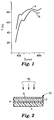
- Light transmissive as used with regard to conductive oxide films, generally includes films which, at a thickness of about 5000 ⁇ , are characterized as being capable of transmitting a majority of incident light between wavelengths of 500 and 800nm. Some light transmissive oxide films of this thickness are capable of transmitting 80 to 90% of incident light between the wavelengths of 600 and 700nm and, while most will transmit a majority of incident light between 400 and 500nm, the transmissivity of many oxide films will decrease dramatically below 500nm (see Fig. 1).
- the light transmissive characteristics of a film can be measured by a Lambda 9 spectrophotometer commercially available from Perkin-Elmer Co. This apparatus provides transmission, reflection, and absorption data in the wavelength range from 200 to 1000nm.
- a "sputtering target,” used in the process of sputtering is comprised of a metal or metal oxide material which, upon sputtering, produces precursors that are deposited as a film onto a substrate.
- Figure 1 is a graph comparing the approximate transmissivities of SnO2:Sb (Denoted by A) and ZnSnO:Al:H:F (Denoted by B) between the wavelengths of about 400 and 800 nm.
- Figure 2 shows an embodiment of the present invention suitable for use as a detector device.
- Light transmissive, electrically-conductive oxides useful in the practice of the present invention comprise tin and a Group II element and are doped with a Group III element and at least one element selected from the group consisting of hydrogen and fluorine.
- a Group III element and at least one element selected from the group consisting of hydrogen and fluorine.
- zinc is the preferred Group II element
- other Group II elements, particularly cadmium would work as well.
- the Group II element may comprise a mixture of zinc and cadmium, with the weight ratio of Zn:Cd being in the range from 1:50 to 50:1.
- a preferred weight ratio of Sn:Group II element is in the range from about 1:20 to 20:1, and is most preferably in the range from about 1:10 to 1:1.
- Group III elements suitable in the practice of the present invention include Al, B, In, Ga, Tl, and mixtures thereof, with the preferred Group III elements being Al and B. If the Group III element is a mixture of Al and B, then the preferred weight ratio of Al:B is in the range from about 1:20 to 20:1. The preferred weight ratio of Al, B, or mixtures thereof to (Group II element+Sn) is less than 3:100.
- Hydrogen can be included as a dopant in the present invention to enhance and stabilize the electrical properties of the oxide.
- Hydrogen can be included according to the atomic ratio H:(Group II+Sn) within the preferred range from about 0.0001 to 0.1 and most preferably within the range from about 0.001 to 0.02.
- H:(Group II+Sn) within the preferred range from about 0.0001 to 0.1 and most preferably within the range from about 0.001 to 0.02.
- hydrogen dopant can be used alone.
- hydrogen in combination with F provides for even further stabilizing of the properties of a transparent, electrically-conductive oxide film.
- the hydrogen and fluorine are preferably present in any H:F ratio from about 1:50 to 50:1.
- the desired atomic ratio of F: (Group II element+Sn) is in the range from about 0.0001 to 0.1, and the most preferred range is from about 0.001 to 0.02.
- Transparent conductive oxide films have been produced by several known processes. See L. Vasanelli, A. Valentini and A. Losacco, Preparation of Transparent Conducting Zinc Oxide Films by Reactive Sputtering , 16 Solar Energy Materials 91 (1987) (evaporation, spray pyrolysis, and sputtering used in production of zinc oxide films); Sarah R. Kurtz and Roy G. Gordon, Transparent Conducting Electrodes on Silicon , 15 Solar Energy Materials 229 (1987) (using atmospheric pressure chemical vapor deposition to deposit a fluorine-doped tin oxide film onto silicon).
- the light transmissive, electrically-conductive oxides of the present invention can be deposited as films upon suitable substrates or energy-sensitive materials by suitable thin film deposition techniques.
- Useful substrates are, for example, glass and flexible substrates such as polyimide, KAPTONTM (from DuPont), Mylar polyester, stainless steel and others.
- substrate also includes energy sensitive materials which function as a component of a detector device.
- a post-deposition annealing step at temperatures up to or exceeding 400°C is desired, low-cost glass, flexible stainless steel, or other materials which are thermally stable at or above this temperature can be used as substrates.
- useful substrates may or may not be stable at temperatures exceeding the temperature at which deposition takes place.
- the oxide film is deposited onto the substrate at a thickness sufficient to provide adequate electrical conductivity and transmissivity for use in optoelectronic devices. This conductivity is measured as sheet resistance, which is a function of film thickness. Generally a greater film thickness will provide a lower sheet resistance.
- the preferred thickness of the inventive oxide films is in the range from about 5000 ⁇ to 1 micron.
- Useful techniques for depositing the inventive oxide films are, for example, sputtering, reactive sputtering, chemical vapor deposition, plasma-enhanced chemical vapor deposition, E-beam evaporation, and laser evaporation.
- the oxides form on the substrate as a film having a granular morphology.
- the size of individual grains is related to deposition temperature, and can be measured by using a scanning electron microscope.
- Deposition of the film by any technique preferably occurs at a temperature sufficient to cause formation of a film having optimal grain size.
- An optimal grain size is a grain size large enough to provide a film having sufficient electrical conductivity, but not too large to reduce the film's transmissivity.
- conductivity and transmissivity are highly dependent on the composition of an oxide, generally a grain size of less than 200 ⁇ will provide inadequate electrical conductivity. On the other hand, at a larger grain size (greater than 1 micron), the transmissivity of the film will suffer.
- the light transmissive, electrically-conductive oxide films of the present invention can be deposited by sputtering suitable targets to produce precursors which will then be deposited onto a substrate.
- Sputtering can be carried out in an atmosphere of a gaseous and vaporous mixture (sputtering gas).
- the sputtering gas can be made up of an inert gas, a hydrogen-containing gas, a fluorine-containing gas and optionally O2 or a Group III dopant-containing gas.
- the hydrogen-containing gas can be H2O vapor or H2 or a mixture of H2O vapor and H2.
- the inert gas is at least one inert gas such as argon, xenon, krypton, helium, or nitrogen.
- Suitable fluorine-containing gases are gases which comprise fluorine, such as C2F6, HF, CF4, CF3Br, hexafluoropropene, fluorocarbons and nitrogen trifluoride or mixtures
- Reactive sputtering is the process of sputtering a metal target in the presence of gases, for example O2, hydrogen-containing gases, fluorine-containing gases, and Group III element-containing gases.
- gases for example O2, hydrogen-containing gases, fluorine-containing gases, and Group III element-containing gases.
- the oxygen is a necessary component of the sputtering gas, because it will react with the sputtered metal target and form an oxide film.
- a preferred metal target for reactive sputtering is Sn/Zn, and the sputtering preferably occurs at a temperature of 250°C in the presence of argon.
- a preferred hydrogen-containing gas is H2
- a preferred fluorine-containing gas is CF4.
- the gaseous mixture can include different concentrations of O2 gas.
- the gaseous mixture includes sufficient O2 to react with the sputtered metal to form an oxide film derived from the metal precursor, the gaseous oxygen, and optionally, other elements comprising the sputtering gas.
- the sputtered target is a metal oxide
- the amount of O2 needed in the sputtering gas is much smaller. Some amount of O2 is preferred even when the precursor is a metal oxide because a small amount of oxygen will be needed to control the stoichiometry of the oxide films.
- Group III element dopants can be introduced for deposition into the oxide film either by inclusion of the Group III element as a dopant in the target or by means of Group III dopant-containing gases being present in the sputtering gas.
- useful gases are, for example, B2H6, B2F6, and BF3, or mixtures thereof, with B2H6 being preferred.
- useful gases are, for example, tri-methyl or tri-ethyl aluminum or mixtures thereof.
- useful gases are indium-containing gases, for example, diethyl indium and dimethyl indium or mixtures thereof.
- useful gases are gallium-containing gases, for example triethyl gallium and dimethyl gallium or mixtures thereof.
- Sputtering targets suitable for producing the light transmissive, electrically-conductive oxides of the present invention can comprise tin and a Group II element, and can optionally be doped with a Group III element.
- the target comprises tin and ZnO and is doped with a Group III element such as aluminum.
- Suitable oxide targets include commercially available oxide targets such as SnO2, or CdSnO4, as well as either ZnSnO, or CdO with Sn, doped with any Group III element useful in the practice of the present invention.
- the particular substrate used in the practice of the present invention can vary widely and can be one of any materials which are useful as substrates for light transmissive, electrically-conductive oxide films.
- the light transmissive, electrically-conductive oxide films of the present invention can be sputtered onto a polymer web to form a polymer sheet with a conductive metal oxide surface.
- the polymer web can be, for example, a polyimide such as KAPTONTM from Dupont.
- the light transmissive, electrically-conductive oxide films of the present invention can be deposited to form a transparent electrode in devices such as photovoltaic devices, photodiodes, radiation detectors, and liquid crystal displays.
- the film can be deposited, for example, onto a glass substrate, or alternatively, the film can be deposited directly onto a layer of energy sensitive material.
- a sputtering apparatus which has been found to be particularly useful in the practice of the present invention is the Perkin-Elmer Model 2400 Sputtering System.
- This apparatus consists basically of an air tight sputtering chamber which encloses an anode where the substrate will be mounted, a target acting as a cathode, and a shield to direct sputtered material toward the substrate.
- a power supply with a radio frequency of 13.56 MHz is connected to the cathode and the anode.
- Gas delivery lines deliver the sputtering gas to the sputtering chamber.
- the sputtering process consists of an initial pumpdown of the sputtering chamber, a presputtering step, which effectively cleans the target, and finally the actual sputtering deposition step.
- the sputtering chamber is evacuated to a pressure of 10 ⁇ 3 torr using a mechanical pump.
- a diffusion pump is used to evacuate the chamber to about 10 ⁇ 6 or 10 ⁇ 7 torr and then the system is filled with the sputtering gas at a pressure of 7 mTorr.
- presputtering occurs for approximately 30 minutes before the actual sputtering deposition step is begun.
- the substrate temperature can be any temperature which allows the gaseous and vaporous mixture to be deposited upon the substrate at an optimal grain size.
- An optimal grain size will produce a film having an acceptably low resistivity, in combination with an acceptably high transmissivity.
- the substrate temperature is within the range between ambient temperature (25°C) and 350°C, and most preferably the substrate temperature is about 250°C.
- the preferred sputtering gas comprises a mixture of argon and hydrogen gases, including H2 at a concentration of about 5%.
- This mixture can be used in combination with a fluorine-containing gas, preferably CF4.
- Alternative gas and vapor combinations which are useful are H2O vapor in combination with C2F6 or HF in N2.
- the gases can be fed into the chamber separately, but they are preferably mixed and fed into the chamber in a single sputtering gas stream.
- the flow rate of this single gas stream can be about 30 standard cubic centimeters per minute (sccm) to give a film deposition rate of about 1A/sec, when sputtering a 10" diameter target at a power setting of 300 watts
- thermal chemical vapor deposition Another method of producing the inventive light transmissive, electrically-conductive oxide films is thermal chemical vapor deposition, or "thermal CVD.”
- thermal CVD can be done at a faster rate and more uniformly over a larger area in order to produce a more uniform product in a more cost effective manner than is possible by sputtering.
- Thermal CVD in terms of practicing the present invention is accomplished by initially producing a mixture of gases and vapors comprising an inert carrier gas, such as nitrogen or argon, and the elements of the oxide film to be deposited. Next, the mixture of gas and vapor is exposed to a heated furnace containing a heated substrate. The gases decompose inside the heated oven and are deposited onto the heated substrate in the form of a film. The temperature of the heated substrate is preferably in a range suitable to produce a film having optimal grain size. An optimal grain size will produce a film having an acceptably low resistivity in combination with an acceptably high film transmissivity.
- an inert carrier gas such as nitrogen or argon
- the gas and vapor mixture can comprise an inert carrier gas, a tin-containing compound, a Group II element-containing compound, an oxygen-containing compound, a Group III element-containing compound, and a H2 gas and/or a fluorine-containing compound.
- the deposited oxide film is derived from the recited gas and vapor mixture, and preferably comprises tin and a Group II element, and is preferably doped with a Group III element, and one or more of hydrogen and fluorine.
- the useful Group II element-containing compounds are, for example, diethyl zinc, dimethyl zinc, triethyl zinc and trimethyl zinc or mixtures thereof.
- Useful tin-containing compounds are, for example tetramethyl tin, tetraethyl tin, dibutyl tin, dimethyl tin, tin dichloride, tin trichloride, and tin tetrachloride or mixtures thereof.
- Useful oxygen-containing compounds are, for example O2, H2O, and volatile alcohols or mixtures thereof.
- Useful volatile alcohols are, for example, isopropanol, ethanol, methanol, etc.
- the fluorine-containing compound can be chosen from the group including HF dispersed in N2, HF dispersed in Argon, CF3Br, and C2F3Br.
- Useful Group III element-containing compounds are, for example diethyl aluminum, B2H6, B2F6, and BF3 or mixtures thereof.
- tin tetrachloride (SnCl4) is mixed with an inert gas such as Ar or N2, which also contains a small amount of H2.
- HF is mixed with an inert gas, such as N2, as a fluorine source.
- a preferred Group II element-containing compound is diethyl zinc.
- a source of a Group III dopant such as boron can be B2H6 or B2F6. Water vapor can be used for the oxygen source, which can be obtained by means of bubbling Ar or N2 through a container of water.
- the process of thermal CVD can be carried out either at atmospheric pressure, or at a reduced pressure (any pressure below atmospheric pressure).
- the gas and vapor mixtures can be combined at a total pressure of about 1 Torr.
- the mixture of gas and vapor flows over the surface of a substrate, the substrate being heated to a temperature sufficient to allow deposition of the chosen gas and vapor mixture onto the substrate as a coated film having optimal grain size, as described above.
- the preferred temperature range for the substrate is between 80°C and 400°C.
- the preferred reactants of tin tetrachloride, diethyl zinc and either B2H6 or B2F6 the preferred temperature range is between 100°C and 350°C. If a thermally-sensitive substrate is chosen, then the preferred reactants comprising the gas and vapor mixture should be chosen to exhibit appreciable reactivity at appropriately low temperatures.
- the inventive light transmissive, electrically-conductive oxides can be formed by means of plasma-enhanced chemical vapor deposition.
- Plasma-enhanced CVD is similar to thermal CVD except that instead of using a heated furnace, a radio frequency (RF) power source is used to excite the plasma and to break up the referenced gases and vapors.
- RF radio frequency
- the RF frequency can be anywhere within the range from 60 HZ to as high as 2.56 GHz.
- a standard RF frequency is 13.56 MHz.
- a post-deposition annealing step can be utilized to eliminate the presence of hydrogen and/or fluorine dopants during the deposition process, and at the same time enhance the crystallinity of the grains in the oxide films and adjust the grain size.
- a process which includes a post-deposition annealing step can be accomplished by a multiple-step sequence.
- the first step is to deposit on a substrate, by means of a suitable thin film technique, a light transmissive, electrically-conductive oxide film comprising tin and a Group II element, the oxide film being doped with a Group III element.
- the second step is to anneal the oxide film in an atmosphere comprising hydrogen and/or fluorine at a process temperature sufficient to produce a film having optimal grain size, as described above.
- the annealing temperature is within the range from 100°C to 400°C, and most preferably the annealing temperature is around 350°C.
- an oxide film can be deposited by a thin film technique, and subsequently annealed in a plasma which contains hydrogen and/or fluorine at a process temperature sufficient to produce a film having optimal grain size.
- the process temperature is within the range from 100°C to 400°C, and most preferably the process temperature is 350°C.
- the light transmissive, electrically-conductive oxide films of the present invention can be useful as electrodes in many applications within, for example, radiation detectors and photosensor devices.
- the advantageous properties of the oxide film, as applied in the form of a transparent, conductive oxide layer, are high transparency and transmission of light for a given thickness, low resistivity, and stability of these properties over time. Since the absorption coefficient of the inventive oxides is relatively small, they can be used to make relatively thicker films, e.g., for use as electrodes, which will have reduced electrical sheet resistance, but without a corresponding reduction in light transmission.
- Photosensor devices and radiation detectors (detector devices) of the present invention comprise a class of devices having an energy-sensitive film with two major sides, the film being made of material capable of generating an electrical signal upon exposure to light or other forms of radiation energy.
- Figure 2 shows part of a detector device 12 , comprising an energy-sensitive layer 2 , a substrate 4 , a first electrical contact 6 , and a second electrical contact 8 , each contact being in electrical contact with a major side of the energy-sensitive film.
- At least one of the electrical contacts 6 or 8 is a light transmissive, electrically-conductive oxide film comprising tin and a Group II element, said oxide film being doped with at least one Group III element, and with dopants chosen from the group consisting of hydrogen and fluorine or mixtures thereof.
- Electromagnetic radiation rays (visible light, x-rays, etc.), 10 , pass through the light transmissive, electrically conductive oxide film, 8 , and strike the energy-sensitive layer , 2 , causing the energy-sensitive layer, 2 , to generate an electrical signal.
- x-rays can pass through a phosphor layer (not shown) which generates light, the generated light then passes through oxide film 8 , and strikes layer 2 .
- An external circuit, (not shown), and connecting means (not shown) for connecting the electrical contacts 6 , 8 , to the external circuit, can be included as part of the device.
- Preferred energy sensitive films are, for example any of the following: a single layer of photoconductive material; a combination of three layers of semiconductors, including a p-type semiconductor, an intrinsic layer, and an n-type semiconductor; or a combination of a semiconductor layer (p-type or n-type) and a metal layer.
- Useful photoconductive materials are, for example, amorphous selenium, cadmium telluride, cadmium selenide, cadmium sulfide, mercury cadmium telluride, selenium-based alloys, telluride-based alloys, selenium telluride, hydrogenated amorphous silicon and alloys thereof and other materials known in the art to be sensitive to electromagnetic radiation.
- Useful semiconductor layers (n-type, p-type, and intrinsic) are, for example, hydrogenated amorphous silicon, or alloys thereof.
- the thickness of the energy-sensitive layer may vary. For example, if the energy-sensitive layer is sensitive to visible light, the thickness can be in the range from 0.3 ⁇ m to 2 ⁇ m, and is preferably in the range from 0.6 ⁇ m to 1 ⁇ m. If the energy-sensitive layer is sensitive to radiation energy, the thickness of the photoconductive layer can be in the range from 50 microns to 1000 microns, and is preferably in the range from 200 microns to 500 microns.
- a light transmissive, electrically-conductive zinc-tin oxide film doped with hydrogen, fluorine, and aluminum, ZnSnO:H:F:Al was prepared using a reactive sputtering method.
- a second light transmissive, electrically-conductive zinc-tin oxide film, ZnSnO:H:Al was prepared in the same manner, to be identical to Compound A with the exception that Compound B was not doped with fluorine.
- a Perkin Elmer Model 2400 Sputtering System was used to produce samples of each of compounds A and B.
- the system had a single deposition chamber equipped with a 13.56 MHz RF power source, a mechanical pump and a diffusion pump with a liquid nitrogen trap.
- the target was a disc 25.4 cm (10 in) in diameter comprising ZnO doped with about 1 weight % Al and mounted on a copper base.
- the ZnO was supplied by Demetron, Inc. of Sunnyvale, California.
- the target further comprised a Sn pellet about 2.54 cm (1 in) in diameter and 0.1 cm thick, which was prepared by melting Sn powder in a steel mold at 400°C. After cooling, the pellet was removed from the mold and mounted onto the ZnO target, near its center, using silver paste EPOTEK H20E from Epoxy Technology Incorporated.
- Substrates (plates of Corning Glass #7095, 5.08 cm x 5.08 cm (2"x2")) were mounted on a rotatable platform inside the sputtering chamber.
- the sputtering chamber was evacuated first by mechanical pump to a pressure of about 1 x 10 ⁇ 3 torr. This was followed by evacuation using a diffusion pump for approximately 2 hours to a pressure of approximately 2 X 10 ⁇ 6 torr.
- sputtering was conducted for 60 minutes by running the system at operating conditions with the shutter closed so that sputtered material was prevented from being deposited on the substrates.
- the sputtering process was then carried out at room temperature (25°C) with 0.60 W/cm2 target power density to give a deposition rate of 1 A/sec.
- a sputtering gas comprising a mixture of Ar and H2 at a flow rate of 50 sccm and CF4 at a flow rate of 1 sccm was introduced into the chamber to give 7 x 10 ⁇ 3 torr of sputtering gas.
- the Ar-H2 mixture available with ultra high purity from Matheson Gas Co., comprised 5% H2 by volume.
- the CF4 flow was adjusted to give a CF4:H2 flow ratio of 0.5.
- the gas flow comprised only the Ar-H2 mixture at a flow rate of 50 sccm.
- each of the resulting oxide films of Compound A and Compound B was 5000 A thick.
- each as-deposited film was measured for sheet resistance at room temperature using an ohm-meter.
- the films were then placed in an oven containing air at 180°C for 60 hours. The films were removed periodically and the electrical resistance was measured. The results of those measurements are shown in the table below.
- Compound A doped with fluorine, showed only minor increases in electrical resistance values over time, while the resistance of Compound B rose rapidly with exposure to heat and air, to values beyond the scale of the ohm-meter (the maximum reading was 108).
- Example 1 the sputtering system and setup of Example 1 was used to produce a Sb-doped tin oxide compound, SnO2:Sb (Compound C).
- the target of example 1 was replaced with a target of SnO2 doped with 3% by weight Sb.
- the sputtering gas was a mixture of oxygen and Argon diluted with 5% H2.
- Sputtering was carried out at a temperature of 25°C to produce an oxide film 5000A thick.
- Figure 1 shows that at a wavelength of 400nm, the transmission of ZnSnO:Al:H:F is about 75% as compared to about 60% for SnO2:Sb.
- Figure 1 further shows that ZnSnO:Al:H:F displays superior transmissivity at all wavelengths between approximately 400nm to 800nm. Further, the as-deposited sheet resistance of SnO2:Sb was 106 ⁇ / ⁇ , or 4 orders of magnitude greater than that of ZnSnO:H:F:Al (Compound A) of Example 1.
Applications Claiming Priority (2)
| Application Number | Priority Date | Filing Date | Title |
|---|---|---|---|
| US217425 | 1994-03-24 | ||
| US08/217,425 US5397920A (en) | 1994-03-24 | 1994-03-24 | Light transmissive, electrically-conductive, oxide film and methods of production |
Publications (2)
| Publication Number | Publication Date |
|---|---|
| EP0675550A2 true EP0675550A2 (fr) | 1995-10-04 |
| EP0675550A3 EP0675550A3 (fr) | 1997-09-03 |
Family
ID=22811030
Family Applications (1)
| Application Number | Title | Priority Date | Filing Date |
|---|---|---|---|
| EP95103453A Withdrawn EP0675550A3 (fr) | 1994-03-24 | 1995-03-10 | Couche d'oxyde transparente à la lumière, conductrice d'électricité, et ses procédés de fabrication. |
Country Status (4)
| Country | Link |
|---|---|
| US (1) | US5397920A (fr) |
| EP (1) | EP0675550A3 (fr) |
| JP (1) | JPH07291628A (fr) |
| KR (1) | KR950033523A (fr) |
Cited By (2)
| Publication number | Priority date | Publication date | Assignee | Title |
|---|---|---|---|---|
| WO2000024686A1 (fr) * | 1998-10-22 | 2000-05-04 | Saint-Gobain Vitrage | Empilement de couches pour substrats transparents |
| WO2014086570A1 (fr) * | 2012-12-06 | 2014-06-12 | Saint-Gobain Glass France | Vitre dotée d'au moins une couche de protection contenant de l'oxyde d'étain et de zinc |
Families Citing this family (38)
| Publication number | Priority date | Publication date | Assignee | Title |
|---|---|---|---|---|
| US5723348A (en) * | 1994-04-25 | 1998-03-03 | Canon Kabushiki Kaisha | Method of making a light-emitting device |
| US5703436A (en) * | 1994-12-13 | 1997-12-30 | The Trustees Of Princeton University | Transparent contacts for organic devices |
| EP0820644B1 (fr) * | 1995-08-03 | 2005-08-24 | Koninklijke Philips Electronics N.V. | Dispositif a semi-conducteur pourvu d'un element de commutation transparent |
| DE19535068C2 (de) * | 1995-09-21 | 1997-08-21 | Lpkf Cad Cam Systeme Gmbh | Beschichtung zur strukturierten Erzeugung von Leiterbahnen auf der Oberfläche von elektrisch isolierenden Substraten, Verfahren zum Herstellen der Beschichtung und von strukturierten Leiterbahnen |
| US5847410A (en) * | 1995-11-24 | 1998-12-08 | Semiconductor Energy Laboratory Co. | Semiconductor electro-optical device |
| JPH09260695A (ja) * | 1996-03-19 | 1997-10-03 | Canon Inc | 光起電力素子アレーの製造方法 |
| US5849108A (en) * | 1996-04-26 | 1998-12-15 | Canon Kabushiki Kaisha | Photovoltaic element with zno layer having increasing fluorine content in layer thickness direction |
| FR2780054B1 (fr) * | 1998-06-19 | 2000-07-21 | Saint Gobain Vitrage | Procede de depot d'une couche a base d'oxyde metallique sur un substrat verrier, substrat verrier ainsi revetu |
| US6395149B1 (en) * | 1998-06-30 | 2002-05-28 | 3M Innovative Properties Company | Method of making light colored, electrically conductive coated particles |
| US6143405A (en) * | 1998-06-30 | 2000-11-07 | 3M Innovative Properties Company | Light colored, electrically conductive coated particles and composites made therefrom |
| US20020084455A1 (en) * | 1999-03-30 | 2002-07-04 | Jeffery T. Cheung | Transparent and conductive zinc oxide film with low growth temperature |
| JP4165785B2 (ja) * | 1999-05-11 | 2008-10-15 | 横河電機株式会社 | フォトダイオードアレイ |
| JP2001027564A (ja) * | 1999-07-14 | 2001-01-30 | Sony Corp | 光検出装置 |
| US6368470B1 (en) | 1999-12-29 | 2002-04-09 | Southwall Technologies, Inc. | Hydrogenating a layer of an antireflection coating |
| TW465055B (en) * | 2000-07-20 | 2001-11-21 | Univ Nat Yunlin Sci & Tech | Method and apparatus for measurement of temperature parameter of ISFET using amorphous silicon hydride as sensor membrane |
| TW468233B (en) * | 2000-09-16 | 2001-12-11 | Univ Nat Yunlin Sci & Tech | Apparatus and measurement method of hysteresis and time shift for ISFET containing amorphous silicon hydride sensing membrane |
| JP4229606B2 (ja) * | 2000-11-21 | 2009-02-25 | 日本板硝子株式会社 | 光電変換装置用基体およびそれを備えた光電変換装置 |
| US6761986B2 (en) * | 2001-04-06 | 2004-07-13 | Rockwell Scientific Licensing, Llc | Thin film infrared transparent conductor |
| EP1289025A1 (fr) * | 2001-08-30 | 2003-03-05 | Universite De Neuchatel | Procédé de dépot d'une couche d'oxyde sur un substrat et cellule photovoltaique utilisant ce substrat |
| JP2003107243A (ja) * | 2001-09-18 | 2003-04-09 | Internatl Business Mach Corp <Ibm> | 光透過膜、該光透過膜の製造方法、配向膜並びに該配向膜を含む液晶パネルおよび表示装置 |
| TWI242053B (en) * | 2002-03-01 | 2005-10-21 | Ind Tech Res Inst | Low temperature method for producing ultra-planar indium tin oxide (ITO) |
| US7189992B2 (en) | 2002-05-21 | 2007-03-13 | State Of Oregon Acting By And Through The Oregon State Board Of Higher Education On Behalf Of Oregon State University | Transistor structures having a transparent channel |
| EP1658643B1 (fr) * | 2003-08-29 | 2018-11-14 | OSRAM Opto Semiconductors GmbH | Dispositif a semi-conducteur emetteur de rayonnement |
| DE102004040968A1 (de) * | 2004-07-30 | 2006-03-23 | Osram Opto Semiconductors Gmbh | Lumineszenzdiode mit einer reflexionsmindernden Schichtenfolge |
| US20060220023A1 (en) * | 2005-03-03 | 2006-10-05 | Randy Hoffman | Thin-film device |
| JP4805648B2 (ja) * | 2005-10-19 | 2011-11-02 | 出光興産株式会社 | 半導体薄膜及びその製造方法 |
| US7280729B2 (en) * | 2006-01-17 | 2007-10-09 | Micron Technology, Inc. | Semiconductor constructions and light-directing conduits |
| DE102006057747B4 (de) * | 2006-09-27 | 2015-10-15 | Osram Opto Semiconductors Gmbh | Halbleiterkörper und Halbleiterchip mit einem Halbleiterkörper |
| US7601558B2 (en) * | 2006-10-24 | 2009-10-13 | Applied Materials, Inc. | Transparent zinc oxide electrode having a graded oxygen content |
| US20100003511A1 (en) * | 2008-07-03 | 2010-01-07 | University Of Florida Research Foundation, Inc. | Transparent conducting electrode |
| US20110083724A1 (en) * | 2009-10-08 | 2011-04-14 | Ovshinsky Stanford R | Monolithic Integration of Photovoltaic Cells |
| KR20110096680A (ko) * | 2010-02-23 | 2011-08-31 | 엘지이노텍 주식회사 | 발광 소자, 발광 소자 제조방법 및 발광 소자 패키지 |
| US20110259413A1 (en) * | 2010-04-21 | 2011-10-27 | Stion Corporation | Hazy Zinc Oxide Film for Shaped CIGS/CIS Solar Cells |
| TWI402370B (zh) * | 2010-06-11 | 2013-07-21 | Ind Tech Res Inst | 濺鍍含高蒸氣壓材料之鍍膜的方法與裝置 |
| US8525019B2 (en) | 2010-07-01 | 2013-09-03 | Primestar Solar, Inc. | Thin film article and method for forming a reduced conductive area in transparent conductive films for photovoltaic modules |
| JPWO2012050186A1 (ja) * | 2010-10-14 | 2014-02-24 | 株式会社カネカ | 結晶シリコン系太陽電池の製造方法 |
| US8476105B2 (en) | 2010-12-22 | 2013-07-02 | General Electric Company | Method of making a transparent conductive oxide layer and a photovoltaic device |
| KR20140128789A (ko) * | 2013-04-29 | 2014-11-06 | 삼성디스플레이 주식회사 | 유기 발광 디스플레이 장치 및 이의 제조 방법 |
Citations (4)
| Publication number | Priority date | Publication date | Assignee | Title |
|---|---|---|---|---|
| US4146657A (en) * | 1976-11-01 | 1979-03-27 | Gordon Roy G | Method of depositing electrically conductive, infra-red reflective, transparent coatings of stannic oxide |
| JPS5789266A (en) * | 1980-11-26 | 1982-06-03 | Seiko Epson Corp | Thin film solar cell |
| US4623601A (en) * | 1985-06-04 | 1986-11-18 | Atlantic Richfield Company | Photoconductive device containing zinc oxide transparent conductive layer |
| US5135581A (en) * | 1991-04-08 | 1992-08-04 | Minnesota Mining And Manufacturing Company | Light transmissive electrically conductive oxide electrode formed in the presence of a stabilizing gas |
Family Cites Families (13)
| Publication number | Priority date | Publication date | Assignee | Title |
|---|---|---|---|---|
| US2682927A (en) * | 1951-10-20 | 1954-07-06 | Chester I Leveke | Suspension for tread supporting wheels of endless tread vehicles |
| US3477936A (en) * | 1967-06-29 | 1969-11-11 | Ppg Industries Inc | Sputtering of metals in an atmosphere of fluorine and oxygen |
| US3506556A (en) * | 1968-02-28 | 1970-04-14 | Ppg Industries Inc | Sputtering of metal oxide films in the presence of hydrogen and oxygen |
| DE2930373A1 (de) * | 1979-07-26 | 1981-02-19 | Siemens Ag | Verfahren zum herstellen transparenter, elektrisch leitender indiumoxid (in tief 2 o tief 3 )-schichten |
| GR79807B (fr) * | 1983-02-24 | 1984-10-31 | Cookson Laminox Ltd | |
| US4514437A (en) * | 1984-05-02 | 1985-04-30 | Energy Conversion Devices, Inc. | Apparatus for plasma assisted evaporation of thin films and corresponding method of deposition |
| JPS6264007A (ja) * | 1985-09-17 | 1987-03-20 | 松下電器産業株式会社 | 透明導電膜及びその形成方法 |
| JPH0641753B2 (ja) * | 1986-08-23 | 1994-06-01 | 株式会社高槻電機製作所 | ダイヤフラムエア−ポンプのダイヤフラム拡張支持装置 |
| JP2647840B2 (ja) * | 1986-10-15 | 1997-08-27 | 三洋電機株式会社 | 燃焼器の制御回路 |
| US4968354A (en) * | 1987-11-09 | 1990-11-06 | Fuji Electric Co., Ltd. | Thin film solar cell array |
| US4940495A (en) * | 1988-12-07 | 1990-07-10 | Minnesota Mining And Manufacturing Company | Photovoltaic device having light transmitting electrically conductive stacked films |
| JPH02210715A (ja) * | 1989-02-08 | 1990-08-22 | Nippon Sheet Glass Co Ltd | 二層構造を有する透明導電基体 |
| US4990286A (en) * | 1989-03-17 | 1991-02-05 | President And Fellows Of Harvard College | Zinc oxyfluoride transparent conductor |
-
1994
- 1994-03-24 US US08/217,425 patent/US5397920A/en not_active Expired - Fee Related
-
1995
- 1995-03-10 EP EP95103453A patent/EP0675550A3/fr not_active Withdrawn
- 1995-03-17 JP JP7058751A patent/JPH07291628A/ja active Pending
- 1995-03-18 KR KR1019950005697A patent/KR950033523A/ko not_active Application Discontinuation
Patent Citations (4)
| Publication number | Priority date | Publication date | Assignee | Title |
|---|---|---|---|---|
| US4146657A (en) * | 1976-11-01 | 1979-03-27 | Gordon Roy G | Method of depositing electrically conductive, infra-red reflective, transparent coatings of stannic oxide |
| JPS5789266A (en) * | 1980-11-26 | 1982-06-03 | Seiko Epson Corp | Thin film solar cell |
| US4623601A (en) * | 1985-06-04 | 1986-11-18 | Atlantic Richfield Company | Photoconductive device containing zinc oxide transparent conductive layer |
| US5135581A (en) * | 1991-04-08 | 1992-08-04 | Minnesota Mining And Manufacturing Company | Light transmissive electrically conductive oxide electrode formed in the presence of a stabilizing gas |
Non-Patent Citations (2)
| Title |
|---|
| PATENT ABSTRACTS OF JAPAN vol. 006, no. 173 (E-129), 7 September 1982 & JP 57 089266 A (SEIKO EPSON CORP), 3 June 1982, * |
| SOLAR ENERGY MATERIALS, vol. 20, no. 5 / 06, 1 June 1990, pages 367-379, XP000135047 HARDING G L ET AL: "DC MAGNETRON REACTIVELY SPUTTERED INDIUM-TIN-OXIDE FILMS PRODUCED USING ARGON-OXYGEN-HYDROGEN MIXTURES" * |
Cited By (4)
| Publication number | Priority date | Publication date | Assignee | Title |
|---|---|---|---|---|
| WO2000024686A1 (fr) * | 1998-10-22 | 2000-05-04 | Saint-Gobain Vitrage | Empilement de couches pour substrats transparents |
| US6541133B1 (en) | 1998-10-22 | 2003-04-01 | Saint-Gobain Vitrage | Layered stack for transparent substrates |
| US6783876B2 (en) | 1998-10-22 | 2004-08-31 | Saint-Gobain Vitrage | Layer stack for transparent substrates |
| WO2014086570A1 (fr) * | 2012-12-06 | 2014-06-12 | Saint-Gobain Glass France | Vitre dotée d'au moins une couche de protection contenant de l'oxyde d'étain et de zinc |
Also Published As
| Publication number | Publication date |
|---|---|
| KR950033523A (ko) | 1995-12-26 |
| JPH07291628A (ja) | 1995-11-07 |
| EP0675550A3 (fr) | 1997-09-03 |
| US5397920A (en) | 1995-03-14 |
Similar Documents
| Publication | Publication Date | Title |
|---|---|---|
| US5397920A (en) | Light transmissive, electrically-conductive, oxide film and methods of production | |
| US5135581A (en) | Light transmissive electrically conductive oxide electrode formed in the presence of a stabilizing gas | |
| JP3358893B2 (ja) | ガリウム−インジウム酸化物を含む透明導電体 | |
| US3811953A (en) | Light-transmitting electrically conducting cadmium stannate and methods of producing same | |
| US4423403A (en) | Transparent conductive films and methods of producing same | |
| US4990286A (en) | Zinc oxyfluoride transparent conductor | |
| US20010008710A1 (en) | Transparent conductive film having high transmission in the infrared region | |
| EP1343176A1 (fr) | Film lectro-conducteur, proc d de production, substrat ainsi pourvu, et convertisseur photo lectrique | |
| US6761986B2 (en) | Thin film infrared transparent conductor | |
| US4069492A (en) | Electroluminescent semiconductor device having a body of amorphous silicon | |
| EP1462541B1 (fr) | Procede pour former un film mince. | |
| US5628933A (en) | Transparent conductors comprising zinc-indium-oxide and methods for making films | |
| EP1635361A1 (fr) | Substrat conducteur transparent, procede de production et convertisseur photoelectrique | |
| US5538767A (en) | Method for growing transparent conductive GaInO3 films by pulsed laser deposition | |
| CN102312201A (zh) | 一种Al掺杂的氧化锌透明导电薄膜的制备方法 | |
| JPH0784654B2 (ja) | Ito透明導電膜用スパッタリングターゲットの製造方法 | |
| JP2928016B2 (ja) | 透明導電膜の成膜方法 | |
| KR20120071100A (ko) | 투명 전도막의 제조 방법 및 이에 의해 제조된 투명 전도막 | |
| JP3325268B2 (ja) | 透明導電膜の製造方法 | |
| JPH08227614A (ja) | 亜鉛−インジウム酸化物を含む透明導電体及び薄膜の作製方法 | |
| Sabnis et al. | Heat treatment of DC-sputtered tin dioxide thin films | |
| Sundaram et al. | Deposition and annealing studies of indium tin oxide films | |
| KR880000448B1 (ko) | 투명 도전막 형성법 | |
| Nakazawa et al. | Transparent and conductive cadmium-tin oxide films deposited by atom beam sputtering | |
| Croitoru et al. | Transport and optical properties of transparent conducting films and photovoltaic junctions with polycrystalline silicon |
Legal Events
| Date | Code | Title | Description |
|---|---|---|---|
| PUAI | Public reference made under article 153(3) epc to a published international application that has entered the european phase |
Free format text: ORIGINAL CODE: 0009012 |
|
| AK | Designated contracting states |
Kind code of ref document: A2 Designated state(s): DE FR GB IT NL |
|
| PUAL | Search report despatched |
Free format text: ORIGINAL CODE: 0009013 |
|
| AK | Designated contracting states |
Kind code of ref document: A3 Designated state(s): DE FR GB IT NL |
|
| STAA | Information on the status of an ep patent application or granted ep patent |
Free format text: STATUS: THE APPLICATION IS DEEMED TO BE WITHDRAWN |
|
| 18D | Application deemed to be withdrawn |
Effective date: 19971001 |